Hi.
1. What maximum step in voltage setting is allowed?
From 0V directly to 12V is Ok?
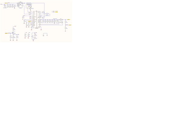
2. In our desing we set 12V Vin and 12V Vout.
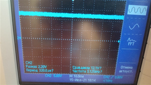
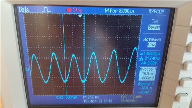
Sometimes after OE Vout has ripple.
If set Vout=0.1V, then set 12V it seems it work fine.
Hi.
1. What maximum step in voltage setting is allowed?
From 0V directly to 12V is Ok?
2. In our desing we set 12V Vin and 12V Vout.
Sometimes after OE Vout has ripple.
If set Vout=0.1V, then set 12V it seems it work fine.