This thread has been locked.

If you have a related question, please click the "Ask a related question" button in the top right corner. The newly created question will be automatically linked to this question.

LM5156: Vout decrease on boost and large Iout condition

Guru 19645 points
Part Number: LM5156

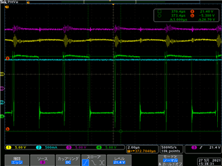
One customer is designing LM5156 on 12Vin ⇒ 24Vout / 2A, schematic is almost the same as below application note Figure-8.

But, when output current over than 1A, output voltage was decrease. (ex. Iout: 500mA ⇒24V, Iout: 1.5A ⇒ about 22V)

Is there any points of the possible to cause, please let me know.

https://www.tij.co.jp/jp/lit/an/snva824/snva824.pdf

Difference point by application note is;

・Vin range: 10V~14V (12V from AC/DC)

・Cin: 10μF

・Cout: 220μF ×1 (Alimnium) + 4.7μF(Ceramic)

・Removed slope compensation (Rs only)

The other parts value is not change.

※Layout and switching current are confirming and requesting to customer. 

Best regards,

Satoshi

  • Hello Satoshi,

    This could be caused by noise injection on the feedback node or into the analog GND.

    Please check as well if the input voltage drops due to the higher output load, then it might be possible that the device runs into the current limit.

    Best regards,
    Brigitte

  • Hi Brigitte

    Thank you for reply,

    I attached waveform for Vout and Switching current, please see below;

    I feel that 300mA and 600mA are not stable, too.

    ※ch1: Switching current (1A/div), ch2: Vout (10V/div), maybe switching current is connected opposite direction the current probe. 

    ・0A ⇒ Vout: 23.5V, 10μs/div

    ・300mA ⇒ Vout: 23.5V, 10μs/div

    ・600mA ⇒ Vout: 23.5V, 10μs/div and 20μs/div


    ・800mA ⇒ Vout: 21.0V, 10μs/div and 20μs/div


    Additional information, I attached switching voltage.

    When start to high-side on timing occur ON/OFF switching.

    And I conscious that FET's gate charge is a little higher than recommend value, is these point have any impact? 

    About layout, I look like feedback node is no problem because of small loop area.

    Now I confirming analog GND.

    Please let me know if you have any notices.

    Best regards,

    Satoshi

  • Hello Satoshi,

    Please check if slope compensation helps. This looks like subharmonic oscillation on the current which would mean slope compensation is needed.

    The loop area for the feedback is seldom a problem. The loop area for the power path and here especially the area transistor, inductor, diode, output capacitor, sense resistor is the most important loop as there are high changing currents.

    Best regards
    Brigitte