This thread has been locked.

If you have a related question, please click the "Ask a related question" button in the top right corner. The newly created question will be automatically linked to this question.

TPS24701: Please review the schematic

Part Number: TPS24701
Other Parts Discussed in Thread: CSD16340Q3, TPS56628

Hello TI experts,

My customer produces the own product since last year, recently they had a problem in the field.

actually we did not check the schematic in development stage.

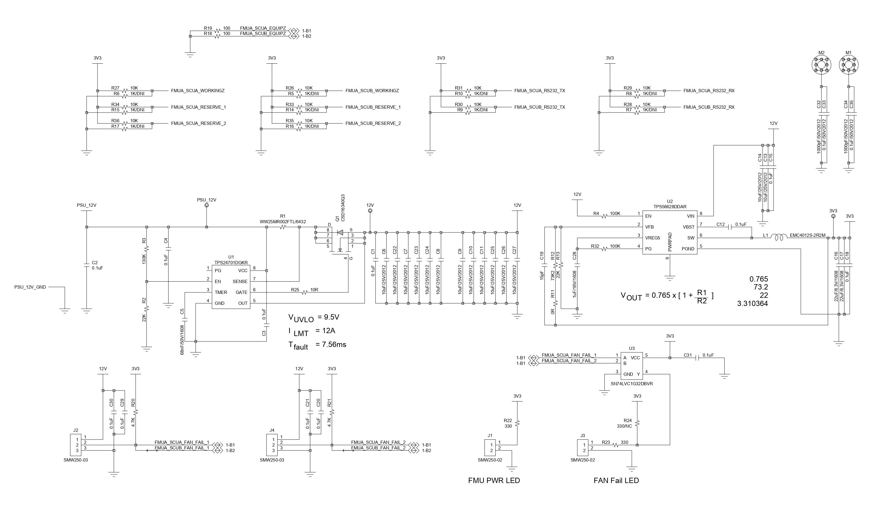
the failure is the dead of Q1 FET, during device running. please check the schematic first.

compare to EVM, i found something differences.

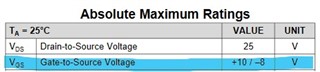
- FET in EVM is CSD16401Q5A, customer's schematic is CSD15340Q3. they have difference in Drain-to-Source On-Resistance. i heard that it causes the heat problem. please confirm that it would be a reason of this failure.

 (also they have difference in maximum SOA.)

- customer do not insert the diodes on input, output and FET_G-S. especially several E2E threads highly recommend to insert zener diode on FET_G-S. please confirm this too, and other diodes if possible.

- and please let me know if you find any possibilities of this failure.

Best regards,

Chase

  • Hi Chase,

    Thanks for reaching out to us. I am reviewing the schematic and will get back to you on Monday. Meanwhile, please could you share the filled up design calculator. It will be helpful for me to review the schematic then. The design calculator is available at https://www.ti.com/lit/zip/slvc567. Please make sure the system specifications, such as output capacitance, load during startup etc. are entered correctly in the design calculator. 

  • Hi Avishek,

    Thank you for your reply.

    I asked to my customer for filling up design calculator. i will send you asap.

    could you give me the result of review even I don't send you design calculator?

    cause it may need little time to fill up that file.

    (I did not inform, voltage is 12V, current is 2.4A constant for every situation.)

    Best regards,

    Chase

  • Hi Chase,

    Did MOSFET get damaged or the Hot Swap controller? At what condition(s) did MOSFET get damaged? MOSFET can be damaged under two conditions.

    1)  MOSFET junction temperature exceeds 150 ⁰C during steady state.

    2) There is a violation in MOSFET SOA during startup or short-circuit events. 

    To evaluate both the above situations, the filled up design calculator is necessary. Please could you share VIN, VOUT, Input Current, and Gate Voltage waveforms just prior to the MOSFET failure. It will help us to identify the root cause of the failure. Suitable TVS diode and Schottky diode are always recommended from transient protection point of view for TPS24701 device. 

  • Hi Avishek,

    Thank you for your reply.

    I did not received design calculator from my customer yet. i will check it again.

    actually it is the damage of MOSFET. after they change it, it works normally.

    and as i said they did not design any diode for their product. do you think it is one of the reason of damaged MOSFET?

    Best regards,

    Chase

  • Hi Chase,

    I think that MOSFET damage is not caused by not incorporating the diodes. I will be sure if you can tell me the condition(s) at which MOSFET got damage. Is this issue repeatable?  

  • Hi Avishek,

    still I am requesting design calculator.

    so do you think that it is the problem of exceeding junction temperature or violation in MOSFET SOA?

    if the customer use the IC that have higher junction temperature and better SOA area, would they prevent the problem?

  • Hi Chase,

    1) so do you think that it is the problem of exceeding junction temperature or violation in MOSFET SOA? Avishek: May be, to make it assured, waveforms and design calculator are necessary.

    2) if the customer use the IC that have higher junction temperature and better SOA area, would they prevent the problem? Avishek: Design calculator is required to confirm.

  • Hi Avishek,

    :: May be, to make it assured, waveforms and design calculator are necessary.

    => do you need the waveforms of just not-operating situation? please give me the points which the waveform needed.

    if you need the waveform of the exact moment of fail situation start, then it would be very hard cause we cannot reproduce the failure yet.

    Best regards,

    Chase

  • Please could you share VIN, VOUT, Input Current, and Gate Voltage waveforms just prior to the MOSFET failure. How many times did this MOSFET failure occur?

  • Hi Avishek,

    Thank you for your reply. i will request these things to my customer, and send you asap. Thanks.

    Best regards,

    Chase

  • Hi Avishek,

    Here is the design calculator. but some information is unclear. please check it.

    - Rds_on_Max : the condition shown is Vgs=10. Id=40A. but in datasheet there is only Id=20A condition. anyway I wrote in Id=20A.

    - FET Gate Charge to reach Vgs>Vta (single FET) : I just wrote same position which figure 2 informed.

    - Retry? : I think we use TPS24701 so the answer is Yes, but if i choose it some calculations are weird.

    - Iramp : I don't know exact meaning of this.

    - T_margin, Minimum Recommended SOA margin : it is definitely up to the customer, but customer have difficulty to determine these values.

    - ENRise : I don't know exact meaning of this.

    and one more thing from customer.

    this failure occurred on running situation, not start or fail time. so i think we don't need to focused on SOA margin, even we have to check it.

    please check this design calculator first. Thanks.

    TPS2470x_Design_Calculator_DAYOU.xlsx 

    Best regards,

    Chase

  • Hi Chase,

    Thanks for sharing the design calculator. I will go through it and get back to you tomorrow. 

  • Hi Chase,

    As the MOSFET failure occurred during steady state, I am suspecting that the issue is due to the lower absolute maximum rating of gate to source voltage of CSD16340Q3, which is +10 V/-8 V.

    GATE pin of TPS24701 can reach maximum to 28 V with input voltage of 12 V when the GATE is fully enhanced.

    Hence, in this case VGS becomes 16 V, which is beyond the absolute maximum rating of CSD16340Q3. Therefore, the MOSFET may get damaged. To eliminate this issue, a suitable Zener diode needs to be placed between gate and source of the CSD16340Q3 as shown in the EVM schematic (D6). BZT52C8V2-7-F may be recommended here as in the EVM schematic. 

    May I know the MOSFET failure occurred multiple times or only once? Is this issue repeatable?

  • Hi Avishek,

    Thank you for your reply.

    May I know the MOSFET failure occurred multiple times or only once? Is this issue repeatable?

    => It occured only once so far. and they did not reproduce it yet.

    1. so do you think it is not the problem of exceeded junction temperature?

    2. How about changing MOSFET same as EVM, CSD16401Q5A, without adding zener diode? is it not a solution?

    3. actually they consider using 2 TPS24701, which load is 1.2A each. (previous schematic is 1 TPS24701 with 2.4A load) could you inform that this solution is suitable?

    Best regards,

    Chase

  • Hi Chase,

    1) I don't think this failure issue is due to exceeding maximum junction temperature. Because, considering maximum current flowing through the CSD16340Q3 of 12 A (ILIM), ambient temperature of 55 ºC, and Junction-to-Ambient Thermal Resistance for CSD16340Q3 as 50 ºC/W, the maximum junction temperature becomes 97 ºC.

    2) CSD16401Q5A can be used instead of CSD16340Q3. However, it's still recommended to keep a place holder for the Zener diode. 

    3) This recommendation is independent of load current. May I know why customer is using TPS24701 for such a low current application? Integrated eFuse is the most cost effective and space optimized solution for this kind of applications, such as TPS2595x.  

  • Hi Avishek,

    I really appreciate for your support.

    I send your opinion to my customer. they review your suggestion now.

    i will reply this thread if there are any updates or further question. Thanks.

    Best regards,

    Chase

  • Hi Avishek,

    finally my customer decided to improve the PCB. could you review this schematic?

    TPS24701_sch2.pdf

    1. they added zener diode in gate-source pin of FET.

    2. they used TPS56628 for generate 3.3V from 12V, now they changed it to voltage divider. (R38 and R39, 26.1K and 10K)

    3. they will put 2 TPS24701 in one PCB, because they want to maintain their system even 1 IC is not working.

    (this application is for cooling fan operation of wired networking system. so cooling fan is important.)

    each TPS24701 will take 1.2A load.

    please check this issue. Thanks.

    Best regards,

    Chase

  • Hi Chase,

    Thanks for following up on this. I will review the schematic and get back to you by tomorrow end of the day.

  • Hi Avishek,

    Please let me know if there are any updates for the issue above. Thanks,

    Best regards,

    Chase

  • Hi Chase,

    Sorry for the delay. I'll get back to you by end of the day today. 

  • Hi Chase,

    Please see the observations in the schematic. 

    1) A suitable TVS diode at input and a Schottky diode at output of the TPS24701 controller are always recommended to place. These two diodes help in protecting the Hot Swap controller due to transient over-voltage at input and under-voltage at output during fast turnoff of the controller. SMCJ18A-13-F and MBRS330T3G may be recommended here as considered in the EVM. 

    2) C1 should be placed as close as possible to the OUT pin of the controller. C2, C3, and C4 should be placed as close as possible to the VCC pin of the controller. This is very important to reduce the effect of noise coming from the fan load. Even another one or two small ceramic capacitors (0.1 - 1 μF) should also be placed at OUT pin along with C1. 

    3) TIMER capacitor (C5) should be 22 or 27 nF to have adequate MOSFET SOA margin during hot short and startup into short events. 

  • Hi Avishek,

    Always thank you for your support.

    I sent your suggestion to my customer. I will reply if I have another question.

    Best regards,

    Chase