This thread has been locked.

If you have a related question, please click the "Ask a related question" button in the top right corner. The newly created question will be automatically linked to this question.

LM25085: Weird behavior at high temps

Part Number: LM25085
Other Parts Discussed in Thread: TPS62135

Hello,

I have included my schematic and layout below.

Vin= 12V-16.8V (4S lithium battery)
Vout= 12V
Full load= 3A
Fsw= ~1MHz

When running a stress test (Full load 3A for a full battery discharge from Vin=16.8V down to Vin=12V), I think the components are getting too hot (probably due to high Fsw). We should be able to solve that issue (reduce Fsw), but I am concerned about how the circuit is acting when hitting this thermal limit. Ideally it would turn off/on with some thermal hysteresis as stated in the datasheet: 170C/150C.

What I see is the output getting stuck in some low output voltage state while still sourcing current. Some details:

  • I recreated the issue with Vin=16.5V and eLoad=3A. It only takes several minutes for the issue to occur. The output voltage falls to ~100mV, eLoad can only sink ~2A (so it's essentially shorting the output trying to get 3A), and input power supply is still at 16.5V sourcing only ~225mA. Thermal camera shows components reaching ~160C.
  • To stop "shorting" the output I reduce the eLoad to 250mA. Output voltage rises to ~700mV and can supply all 250mA of load current. Input voltage still 16.5V and ~200mA. Components still around ~160C. (Fig1,2,3)
  • I disconnect the eLoad completely. Power supply still at 16.5V and ~200mA (where is this current going?). Components still around ~160C. (Fig4)
  • Power cycling the converter restores normal operation.

Some scope captures to expand on these details:

Fig1
Ch2 (purple): PGATE
Ch3 (blue): VOUT
Ch4 (green): VIN
Iin= 200mA
Iout= 250mA
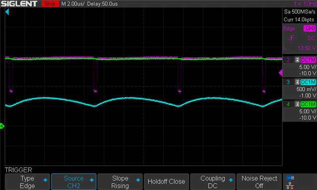
Fig2
Ch2 (purple): SW Node
Ch3 (blue): VOUT
Ch4 (green): VIN
Iin= 200mA
Iout= 250mA


Fig3
Ch2 (purple): SW Node (emphasis on negative voltage during diode conduction)
Ch3 (blue): VOUT
Ch4 (green): VIN
Iin= 200mA
Iout= 250mA

Fig4
Ch2 (purple): SW Node
Ch3 (blue): VOUT
Ch4 (green): VIN
Iin= 200mA
Iout= 0.0A (eLoad disconnected)


L=2.2uH

PFET: DMP2040-UFDF-7
Diode: PMEG3020EGWJ
Inductor: NRS5024T2R2NMGJ
C26 VCC cap has it's polarity reversed in the schematic, but it is ceramic.

Any ideas what is happening?? Thank you very much! I can provide/collect any other info you might need.

  • Hey TI_Lover, we love you too.

    At first glance your type-3 ripple resistor R78 is very small at 6.04kΩ.

    We usually recommend this be in the 100kΩ to 1MΩ range to have high impedance between SW node and FB loop (type-3 ripple caps are low AC-impedance)

    You can size this R78 up 10x to 60.4kΩ and size down C45 to see if that improves response. Let me know if that works.

    You can also reference

    https://www.ti.com/lit/an/snva776a/snva776a.pdf for general guidance on ripple networks

    https://www.ti.com/lit/an/snva874/snva874.pdf which considers output ripple effects on Type-3 networks.  

    Hope this helps,

    -Orlando

  • Another thing to check is the inductor - when operating at hot, the sat current reduces and it may enter saturation and engage current limit (set at 5.8A). Consider changing the inductor to a shielded design. Also, 2.2uH seems very low  for a 3A design, even at 1MHz (ripple is 1.5Apk-pk at 16.5Vin, 12Vout).

    In addition, check the power semiconductors. The FET Qg is 15nC at Vgs = 7.7V. This corresponds to 15mA DC current at 1MHz (min VCC current limit is 20mA). And the diode is only rated for 2A in a relatively small SOD-123 package. Recommendation is to reduce Fsw as already suggested to increase efficiency and lower the operating temperature.

    Please use the LM25085 quickstart calculator to check your design: https://www.ti.com/tool/LM25085-5085QUICK-CALC

    Regards,

    Tim

  • Whoops, never closed this thread...

    As always, really appreciate TI's quick support (and lately, you two engineers especially).

    It will take some time to implement these changes, but I feel confident we will see improvements at lower Fsw. One other thing I noticed was the thermal resistance of the Schottky being used was very high (190C/W). I think we might have been entering a thermal runaway, which I learned can happen with Schottky diodes as their reverse current increases dramatically with temperature. Leaving the Fsw at 1MHz but swapping in a more robust diode has already helped avoid this weird behavior.

    One last piece of feedback: most of the questionable design decisions made here (high Fsw, small packages) was done because this regulator needed to fit in the PCB area once occupied by the TPS62135 (no supply available). It's not east to find buck converters with true 100% duty cycle mode (meaning you don't need to separately bias the bootstrap cap). Would love to see this feature get a unique name that can be searched for in the parametric tables. Just my 2 cents Slight smile

    Anyways, no more actions needed for now. Thanks again.

  • Thanks for the comments and feedback. Yes, diode performance can be impacted at hot due to the large reverse leakage current.

    Regards,

    Tim