


Hi,
We are using 3x UCC27282 in a 3 phase inverter application with the following specs:
- 100V DC Bus, 12V VDD for UCC27282
- 2x parts of MOSFETs in Parallel each with Qg = 120nC. 4x FETS per phase in total.
- 20 KHz PWM driving a outrunner BLDC motor (low inductance).
- 1mR current shunt sense resistor
At voltage levels below 36 VDC our design is stable, and largely free of noise, overshoots, thermal good, etc.
At voltage levels above 36 VDC all of our gate drivers fail simultaneously. When we activate the lower gate driver, the device draws 0.2A / 12V. The device has clearly failed.
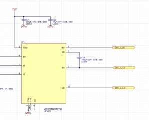
There is nothing special about the gate driver setup as below:
The schematic for our FETS is below. Note: we have U.FL (SMA RF) connectors at all critical points for signal analysis.
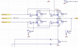
The PCB layout is 4 layers of 2oz copper, very solid.
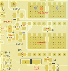
I've annotated the major components as in the image below. For the UCC27282 we have the exposed pad bonded to 4 layers of copper with vias, and the GND pin bonded to a plane with a via directly at it.
C_boot and VDD caps are directly at the pins.
The only real question mark in the design the length of the LO signal between UCC27282 and the LO side gate resistors, however the track length is only 14mm millimetres long.
So we are looking for some suggestions as to what we can test to determine why we have all of our devices with LO side failures at (or about) the same time.
Could the current sense resistor be the cause of our issues? - Could this resistor somehow allow LO to go beyond a specification?.
Is the loop inductance between LO pin and gate resistor a possible source of error? I don't see anything bad on the scope when connected to the SMA at the lower gate resistor.
We notice that in SNVSAQ5A.PDF, section 8.2 (Typical Application) there are Shottky diodes at the LO pin, and between HS and HO. If we need these diodes in our design, how do we determine that?. What is the parameter of the UCC27282 that the diodes are trying to protect?
Could our deadtime somehow contribute to these failures?
Thanks
Stomp!.
