Hi,
I think I need help from someone from TI who is familiar with the inner workings of the controller, or who has already come up against this issue & solved it.
Thanks, in anticipation!!
I'm trying to develop a 350W LLC using this controller.For various reasons we want to minimise the effective series primary inductance.
This means that there is even more of an issue with high primary circuit current in conditions where Vout is low (during startup & abnormal conditions).
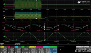
I have a prototype which is showing around 18A peak primary current at startup (Vht = 380V, Vout = low, effective series inductance around 8~10uH, controller runs at ~590kHz)
18A peak is a bit scary for this application, but the controller is not pushing the frequency up to reduce it.
SS pin is low ~0.6V but the VCR pin is showing -0.9V to +7.4V peak-peak, and -0.6V / + 7.0V just before the switching points of the primary switches.
I don't understand why the controller is not commutating sooner, when VCR crosses (effectively) +/- V(SS pin), which I think is what it should be doing in these circumstances
The only explanation I can think of is the propagation delay from VCR crossing the Vth / Vtl thresholds to changing the gate drive (see sect 7.3.1 of the datasheet)
What is this propagation delay likely to be? Is it in the datasheet anywhere, I can't find it?
What are the practical (controller) limits to maximum operating frequency (I note minimum on-time is ~250ns)?
Notes:
cap from VCR to 0V is 2N7
power switches are GaN with very low gate charge, so they'll not be hard to drive fast
The trace shows a burst at low Vout, terminated by OCP2, I think
CH1 Yellow VCR pin of UCC2465404
CH2 Red HB out = TX term 1 in
CH3 blue V(Cres)
CH4 green Ipri
D0 violet HB gate L
regards,
Paul Ryan