This thread has been locked.

If you have a related question, please click the "Ask a related question" button in the top right corner. The newly created question will be automatically linked to this question.

TPS62913: Trace widths

Part Number: TPS62913

Hi, 

I'm looking at using the TPS62913 to provide a 3A 1.35V rail. 

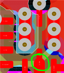
Looking at the land pattern recommendation, the SW node is 0.2mm x 1.0mm. Using online PCB trace calculator tools, it looks like a trace that's only 0.2mm will struggle maintain 3A of current - even with very high plating options. 

Am I right in thinking this land pattern is OK because the pins quickly fan out into large inductor pads? Is there any way to verify this is OK in Webench - I recall there used to be thermal simulation option but this doesn't appear available for this device. 

Any advice would be greatly appreciated. 

Many thanks

  • Hello Pjs,

    Your thinking is correct on the SW pin footprint. My advice is to:

    1.)  Use at least a 0.2mm trace, but make sure its width doesn't have clearance issues with surrounding pins.

    2.) Place the inductor close to the SW pin to reduce trace length (resistance and parasitic inductance).

    3.) Webench should provide junction temperature of the IC for the design under set operating conditions but don't think it allows you to change trace width.

    The datasheet provides a typical layout showing the SW trace to the inductor in Figure 10-1.

    Let me know if this helps.

    Thanks,

    Joseph

  • Hello,

    You are correct, that the SW node trace width and solder mask should be wider than the standard package addendum in the datasheet.  I would recommend following the layout in the EVM design, available on the product page. The footprint will accommodate widening the trace under the part as shown circled below.

  • Many thanks Steve + Joseph!