Because of the holidays, TI E2E™ design support forum responses will be delayed from Dec. 25 through Jan. 2. Thank you for your patience.

This thread has been locked.

If you have a related question, please click the "Ask a related question" button in the top right corner. The newly created question will be automatically linked to this question.

UCC21540: Duty cycle lose

Part Number: UCC21540

Dear technical support:

Hello! We are using TI's UCC21540 device, but there are some questions during the application. Now I want to consult technical support and hope to get your help.

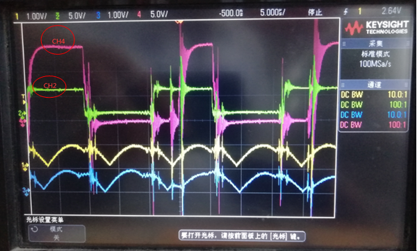
1. Figure 2 in the attachment is the test waveform of INA/B vs. GND for CH2, and the test waveform of OUTA/B for CH4.During the test, when we were at a high temperature of 60℃, the waveforms of the primary side and the secondary side could overlap, but when the ambient temperature rose to 70℃, the waveforms began to appear non-coincidence, and there was a problem of loss of duty cycle. For this reason, I would like to ask what causes this phenomenon? Is there any reasonable solution? thank you for the help!

NOTE: CH2 is the test waveform of INA/B to GND, CH4 is the test waveform of OUTA/B. For screenshot, you can check attachment.

UCC21540.pdf

  • Hi Lidong Yu, 

    Thank you very much for reaching out through E2E. 

    I am trying to get more information for this issue in order to better understand the root causes for this problem you are observing. 

    1- Can you provide a full schematics for your system? 

    2- Do you have waveforms separating INA and INB, and OUTA and OUTB. I would like to see these measurements separately. 

    3- Can you also provide measurements for VDDx rails? Are you supplies stable ? 

    Sincerely,

    Francisco Lauzurique  

  • 1- Can you provide a full schematics for your system?

    Repel: The schematic diagram is as follows:

    2- Do you have waveforms separating INA and INB, and OUTA and OUTB. I would like to see these measurements separately.

    Repel: INA, INB, we haven’t tested the waveform yet

    3- Can you also provide measurements for VDDx rails? Are you supplies stable ?

    Repel: We have checked VDD and the power supply is stable. For the purchase channels of our UCC21540 devices, we are looking for a reliable way to buy, and there will be no fakes. Regarding the issues we consulted, what aspects of your preliminary analysis may cause the issues?

  • Hi Lidong, 

    Thank you very much for sharing the following schematics for your system. 

    1- Can you share the part number for your bootstrap diode 

    Before beginning to eliminate possible causes for this issue we need to ensure that during the issue, we have the expected operating working conditions for our devices. I am trying to understand how are your input supplies when the issue is happening. I want to ensure that INA/INB are as expected. I noticed that your inputs INA and INB do not have the recommended RC filtering and noises could affect the output. This could lead to the issue we are seeing since you input waveforms have noises as observed in the previous measurements

    In addition, if your supplies are not behaving as expected and are dropping below UVLO in the VDDx supply pin, then we could be observing this issue. Having very noise supplies could affect the OUTx for the driver by cause the driver to miss part of the pulses depending of the frequency you are switching. 

    Can you provide some of these requested measurements so we can begin to eliminate some possible scenarios for these issues

    Sincerely, 

    Francisco Lauzurique  

  • 1. Diode model we use:

    D3 / D4: SS14 (1a / 40V) of ansenmey brand; As attached

    D1:1A/600V/ES1J; As attached

    D3 D4(SS14) (1).pdfD1(ES1J) (1).pdf

    2. Our ina / B has RC filtering. Due to the size limitation of the picture, the RC filter circuit is not effectively displayed in the picture. The RC filter we added is 100 Ω, 1nF.

    3. Our power supply VDDx is reliable. We can work normally under normal temperature and high temperature below 60 ℃.

    4. The ina / b waveforms tested separately are normal. Since the waveform pictures were not saved in time during the initial test, we have not found suitable test data and waveforms temporarily.

  • Hey Lidong,

    If it isn't too much trouble, there are a couple of pieces of information that would be helpful in solving this issue.

    1. Could you provide the plots and/or details of the PWM signals used for INA and INB? Seeing these signals separately would greatly help us assess the issue.

    2. Please confirm the Capacitances of C2, C3, C7, and C8, as shown in the schematic.

    This information should give us a better idea as to the problem at hand.

    Thanks,

    Jacob Cohen

  • 1、The PWM waveform of INA/B is CH2 in the attachment.
    2、C2\C7 capacitance is 10uF, C3\C8 capacitance is 100nF.
  • Hey Lidong,

    I have a couple of ideas that could be leading to your issue.

    1- Are the input pulses overlapping at all? Leaving some dead time in between the input signals could help fix this issue if there is not any implemented currently.

    2- Based on the capacitor values provided, the components of the bootstrap circuitry could be leading to the issue.

    This link leads to a TI document regarding how to ensure the bootstrap components are correct: https://www.ti.com/lit/pdf/slua887.

    Please let me know if either of these ideas were helpful in solving the issue.

    Thanks,

    Jacob Cohen