This thread has been locked.

If you have a related question, please click the "Ask a related question" button in the top right corner. The newly created question will be automatically linked to this question.

TPS55340: PWM regulation does not start at low temperatures -10 ℃

Part Number: TPS55340
Other Parts Discussed in Thread: TPL5110

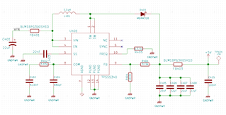
To power our system from a one-cell ion lithium battery a DC/DC regulator based on the Texas Instrument TPS55340 has been designed with the following requirements:

  • Vin: 3.6 ~ 4.2 V
  • Vout: 5 V @ 3A max.

Custom design has been done according to the WEBENCH Power Designer recommendations. Circuit is in production and the system is deployed.

During the process of validation of the devices we have detected an issue during the low temperatures operating cycle (-10 ℃  48 hours). Some of the devices present battery discharges associated with a constant reboot loop of our system.

After the failure analysis, we have been able to conclude that the TPS55340 DC/DC regulator has not started the PWM control although all input signals are correct (input voltage is within range and enable pin is high). When this happens, output voltage is established by a direct connection between the input voltage and the output through the inductor and rectifier diode.

We have observed that PWM regulation starts to work after some minutes (~5min) in ambient temperature. Otherwise, if the device is kept on low temperatures, TPS55340 does not start until Vin is reset to 0 V and power up again. .

This event is aleatory but some devices present the issue more often on the order of 1 event every 24 soft starts.

What could be the cause of this issue? Is it possible that the internal oscillator does not start properly at these temperatures?

Is this IC suitable to work at these low temperatures for long periods of time?

Thanks in advance for your support

Esteve

  • Hi, Esteve,

    Thank you for your careful observation and analysis. To help me understand the issue,

    1. what is the test condition in the low temperature test cycle? Vin=?, Vout=?, Iout=? fs=? do you monitor these parameter all the time during test?

    2. Are there any event (like input/output voltage changing, or other event) or parameter change (like load changing) during the low temperature test except temperature decreases to -10C?

    3. Did this issue happen as soon as temperature drops to -10C? or happen when stay in -10C for some time?

    4. You mentioned that all input signals are correct. Do you mean that all signals are correct after TPS55340 stop working? or all signals are correct during the test procedure of TPS55340?

    Thank you so much.

    Zhiyang

  • Hi Zhiyang

    I'm sensing clarifications. I hope that help you to understand the issue. 

    1. What is the test condition ...

    The normal expected condition of the test follow three stages:

    1. A true-shutdown circuit disconnects V_IN for a period of time of 75 min. True-shutdown circuit corresponds to a TPL5110 that drives the gate of a P-MOS MOSFET.
    2. The TPL5110 timer opens the P-MOS MOSFET, powering the DC/DC regulator. In this stage the V_IN is connected to a Li-ion battery with a voltage range of [3.90 V, 4.0 V]. Target V_OUT is +5V, and expected I_OUT average current is 850 mA with peaks up to 2 A. ƒsw frequency is set by the R_FREQ (47.5 k Ohm) at 983.33 k Hz. We do not monitor the V_IN during the test, because the DC/DC regulator is disconnected and inactive.
    3. A MCU, powered with V_OUT (+5V) carries out the test and sets the TPL5110 DONE signal when the test is done. After the DONE, TPL5110 timer set P MOSFET Drive to high, disconnecting the DC/DC regulator from the power source.

    The issue appears in stage 2, when the TPS55340 DC/DC regulator has not started the PWM control. Without the PWN regulation the V_OUT is equal to V_IN voltage minus the voltage of the Schottky rectifier diode. Without the PWM switching, between the input and the output we have a passive path that can not power the MCU.

    1. Are there any event or parameter change ...

    No, the issue appears in the transition between stages 1 and 2, when the TPS55340 DC/DC regulator is powered after a period of 75 min of true-shutdown circuit disconnection.

    1. Did this issue happen as soon as temperature drops to -10C? ..

    No, the issue appears randomly. We have sequences of successfully soft-start, with sporadic events (failure/success ratio ⅕). The issue appears more frequently in a few devices, the rest works fine and passes the 48 hours test without failure events.

    1. You mentioned that all input signals are correct…

    From a black-box point of view, the input signals V_IN and EN (enable) are correct, and do not change along the test period. Expected outputs are not correct because the PWM regulation does not start.

    Best regards

    Esteve

  • Hi, Esteve,

    Thank you so much for your clarification.

    My understanding is that first TPS55340 board/part stay in -10C for 75 minutes, and then power up to +4Vin by TPL5110 controlled circuit, 4/5 of TPS55340 boards/parts regulate Vout=+5V fine, and 1/5 of TPS55340 boards/parts lost output regulation and results Vout=+~3.7V.

    For the 1/5 TPS55340 boards/parts with Vout=+~3.7V, reset Vin of TPS55340 board/part to 0V then power up and the TPS55340 board/part regulate Vout=+5V fine.

    Basically, both actions above reset Vin=0V for TPS55340 board/parts. What is the major difference between the TPL5110 controlled power up and the second reset Vin=0V and then power up? Could you measure transient waveforms of Vin pin, SS pin, and COM pin?

    BTW, the circuit schematic indicates that GNDPWR and AGND are not separated for the controller chip. And, for pin 6, if it is not used, it should be tied to AGND. For pin 11, it must be connected to AGND by datasheet. 

    Thank you.

    Zhiyang

  • Hi, Esteve,

    How is this case going?

    Thanks.

    Zhiyang

  • We have been repeated the low temperature tests with the NC (pin 11) and SYNC (pin 6) connected to AGND and the DC/DC works fine.

    Please, I suggest to modify the datasheet changing the NC pin name because does not appears in the 7.2 Functional Block Diagram and can be interpreted as Non Connected.

    The error of the SYNC is my fault, datasheet explain than "If not used, this pin should be tied to AGND".

    Thanks for your support.

    Kind regards

    Esteve