This thread has been locked.

If you have a related question, please click the "Ask a related question" button in the top right corner. The newly created question will be automatically linked to this question.

UCC27517: Return path for In-

Part Number: UCC27517
Other Parts Discussed in Thread: SN74LVC1G14

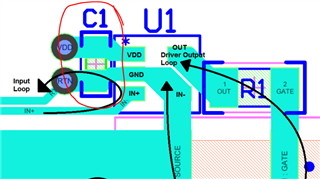
In the screenshot the IN- pin is connected to Gnd. Is it required to route the In- parallel to the IN+ input. The operating speed is 5 MHz.

OUT signal is connected to the Cathode of Optical transmitter and Anode is connected via a Resistor to 5V.

IN signal is driven by a SN74LVC1G14.

Do you think the layout has enough capacity to work at 5MHz with Iout(Sink) 80mA.

  • Hi Deepak,

    Thanks for reaching out!

    -------

    1)  I am a bit confused by the layout; I assume this is flipped upside-down?

    2)  Is it required to route the In- parallel to the IN+ input?:  Unless you are sending differential signals, there should be no need to parallel the traces (Because the IN- is being connected to GND.

    3)  If you want to improve the layout more, consider moving the VDD capacitor across the IC, as close as you can:

    4)  Whether this will okay or not may depend on how hot the driver will get.  This can depend on what the diode capacitance of the optical transmitter is.  Please refer to Section 12.4 of the datasheet along with the thermal considerations such as the thermal resistances.

    Since the diode capacitance will likely be in the tens of pico-Farad range, this should work and not be a concern.  I mentioned statement "4" for peace-of-mind, so you could consider running power dissipation calculations.  The 80mA Iout(sink) should not be an issue either.

    -------

    I hope this helps!  If this answered your question, please press the green button.  Otherwise, feel free to follow up.

    Thanks!

    Aaron Grgurich