This thread has been locked.

If you have a related question, please click the "Ask a related question" button in the top right corner. The newly created question will be automatically linked to this question.

CSD22205L: Suggestion for layout...

Part Number: CSD22205L

Hi Sir,

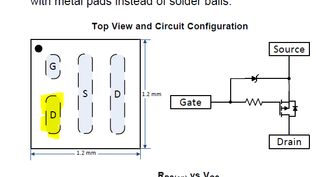
My customer is layout the CSD22205L and got confused.

Here is the layout.

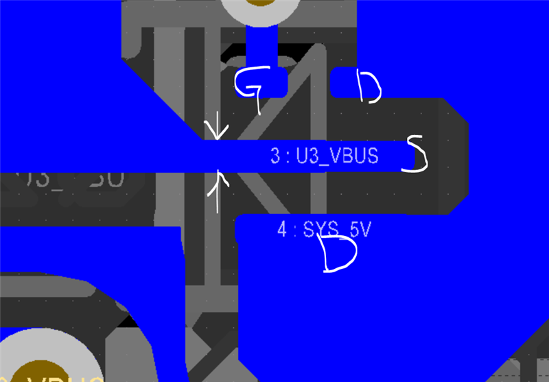
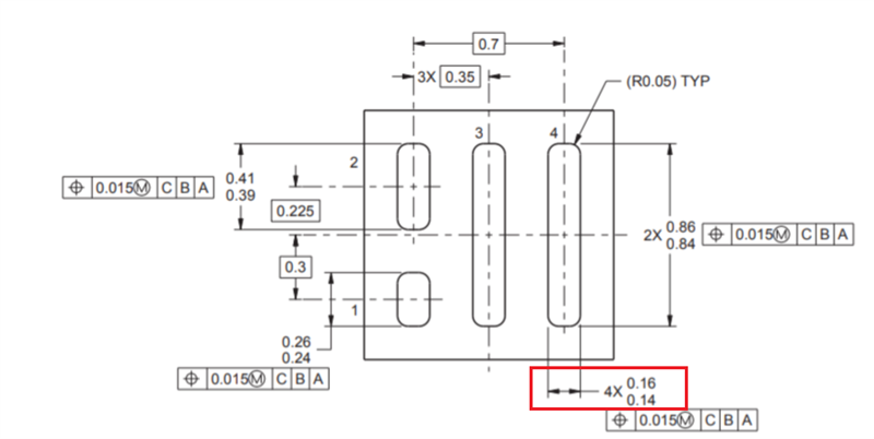
As the source pin trace width, customer worried it cannot support up to 2A.

Is there any layout guide or suggestions for customer layout?

Thanks.

  • Hello Peter,

    Thanks for promoting TI FETs at your customer. Can you verify that the customer is following the PCB land pattern recommendations in datasheet? Are they using solder mask defined or non solder mask define pads? Please ask the customer if they can share their gerber files for TI to review.

    Best Regards,

    John Wallace

    TI FET Applications

  • Hello Peter,

    Additional information requested by our SMT expert below.

    In order to determine if the trace width of “S”
    is sufficient to hold 2A, we will need the following:

    1. This looks a Solder Mask Defined Pad layout.
    2. We will need the copper weight (in oz or thickness)
    3. “S” Trace width
    4. At what temperature the board is running

    Thanks,

    John

  • Dear John,

    Customer feedback as below.

    1. Copper thickness is 18um
    2. "S" trace width is 6 mil = 0.15mm
    3. The temperature will be 20°C to 80°C

    Another question: if the yellow marked "D" pin can be left N.C or not then customer will have more space to route for both side of "S" pin.


  • Hi Peter,

    Thanks for providing additional information. I have passed this onto our SMT expert to get his feedback and will update you as soon as I have more information.From an electrical standpoint, leaving the smaller drain pad open should be OK but the effective on resistance may be slightly higher. It may cause some issues during assembly onto the PCB as distribution of the solder paste will be uneven. I don't know if this might cause the device to tilt during reflow soldering. I will ask our SMT expert for his opinion on this as well.

    Best Regards,

    John

  • Hello Peter,

    Thanks again for promoting TI FETs at your customer. Please see feedback from our SMT expert below.

    Current capacity is a function of cross section area
    and temperature.

    PCB world use mil and oz

    Customer is using 0.5oz copper (0.709 mil) and
    trace width 6 mil.

    Below table is an analysis of current design and how
    to get to 2A at 75C.

    PCB Copper (oz)

    Copper Thickness (mil)

    Trace Width (mil)

    Copper Cross section area   (Sq Mil)

    Max Current at 20C

    Max Current at 30C

    Max Current at 60C

    Max Current at 75C

    0.5

    0.709

    6

    4.254

    0.5

    0.65

    0.75

    1.0

    1

    1.418

    6

    8.508

    0.75

    1.0

    1.3

    1.5

    1.5

    2.127

    6

    12.762

    1.0

    1.3

    1.75

    2.1

    The trace width has to match with the package.

    Only thing they can change is copper contents (thickness).

    Base on this table, in order to carry 2A, the PCB has to use
    1.5oz copper.

    If the small drain is not soldered, there is a risk that
    the package would tilt towards that corner during reflow. TI has not evaluated this configuration.

    Best Regards,

    John