This thread has been locked.

If you have a related question, please click the "Ask a related question" button in the top right corner. The newly created question will be automatically linked to this question.

LM2733: Looking for information on compensation network values.

Part Number: LM2733
Other Parts Discussed in Thread: DRV8860EVM, DRV8860,

I'm having stability troubles with my design for the LM2733XMF. I have been using the Power Stage Designer Tool to create bode plots for my design and analyze the stability. My issue is that I cannot find the values for the internal compensation circuit. The datasheet only shows a functional diagram which does not resemble any of the Power Stage Designer Tool compensation network types. Can anyone give me any guidance on this so I can use the Power Stage Designer Tool effectively with the LM2733XMF?

  • Hi James,

    May I know what kind of specific stability trouble do you have now? Can you share your application's schematic and Vin, Vout, Iout spec? I can help review the schematic for you. Thanks.

  • Hi Zack,

    Here is my specs: Vin = 7V, Vout = 12.8V, Iout =0.3A.

    The design was based off of the DRV8860EVM board and I have attached a picture.

    The stability issues I'm encountering is when there is no load being actuated so this is much below even 0.1A. I'm seeing sometimes the output is not being boosted to the 12.8V and is staying at the same voltage as the input. Once the device enters this state of instability, it cannot recover, even if a load is applied. and requires a power cycle to recover. The circuit below powers two DRV8860 drivers.

  • Hi James,

    From your description, it doesn't seem to be a stability issue. The stability issue normally refer to ringing during load transient or obvious Vout oscillation.

    Can you share the layout of your PCB? 

    May I know in which condition that device could work normally and output 12.8V?

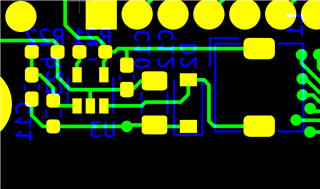
  • Here is the board layout:

    It uses traces instead of polygons but they are pretty short traces so I don't expect too much parasitic inductances.

    I'm not sure what you mean by what condition would it normally operate in. But it will output 12.8V when the two DRV8860s which are the only components using the 12.8V output and are driving either no load or up to 150mA of load.

  • Hi James,

    It's always needed and necessary to use polygons for the power trace: Vin->Inductor->SW pin->Rectifying diode->Vout->GND. Otherwise there would be unexpected problems happening. TI strongly recommend customer to use polygon.

    You mentioned it cannot output 12.8V at no load in previous email. Why you said it will output 12.8V when the two DRV8860s driving either no load or up to 150mA of load?

  • Sorry What I meant was sometimes it fails to produce 12.8V at no load but most of the time it works.

  • Hi James,

    You need to update the layout definitely.

    May I know the failure rate so far? Does the issue follow the PCB or IC? Have you tried solder a new IC on the same PCB and test the board again?

  • I have just finished a new design where I copy the exact recommended board layout as per the LM2733 datasheet. It'll be a while before I get these PCBs back for testing.

    The issue follows the PCB, we're seeing failures anywhere from within the first hour up to 5 days. I haven't swapped out the component on the PCB yet but we're experiencing power failures across all PCBs.

    Thanks,

  • Hi James,

    Could you share your latest layout? I will double check it.

  • Hi Zack, Thanks for reviewing the design here's what I have, let me know if there's anything you would change.

  • Hi James,

    You don't need to pour a wide copper for FB net because it brings bigger parasitic capacitance between FB to GND, which adds a pole in the loop. You can see TI EVM use a short, thin trace for FB net.

    Is there any big GND plane on inner layers or bottom layer? You can add some GND vias close to IC GND pin.

  • Thanks for the tip on the FB trace. Yes there is a whole Ground plane in one of the inner layers as well as the bottom layer. I'll add some vias.