


Dear team ,
In my board design , there are two power supplier 5V and 3.3V . They are not exist at the same time . And 3.3V is the main power for whole board.
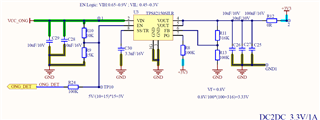
So i use TPS82150 for power conversion : 5V To 3.3V .
But there is a quesion , when only 3.3V for the power supply. The 3.3V is also connect the output pin of TPS82150 , at the same time it generate a 2.7V voltage at input pin of TPS8015.
accroding the datasheet of TPS82150 , there is a inductor and a N-MOS between output pin and input pin. 3.3V voltage throught inductor and body diode of MOS to the input pin .
this is not expect in my design .
Could you please give me some suggestion or other IC schem , picture below is Schematic, thanks .
Kind regards,
kirin
