This thread has been locked.

If you have a related question, please click the "Ask a related question" button in the top right corner. The newly created question will be automatically linked to this question.

LM25184-Q1: Oscillation analysis

Part Number: LM25184-Q1


Hi team, 

My customer is evaluating LM25184-Q1 in their new gen platform. Could you please kindly help comment how to improve below oscillations?

1. The oscillation of secondary diode turning on (in blue)

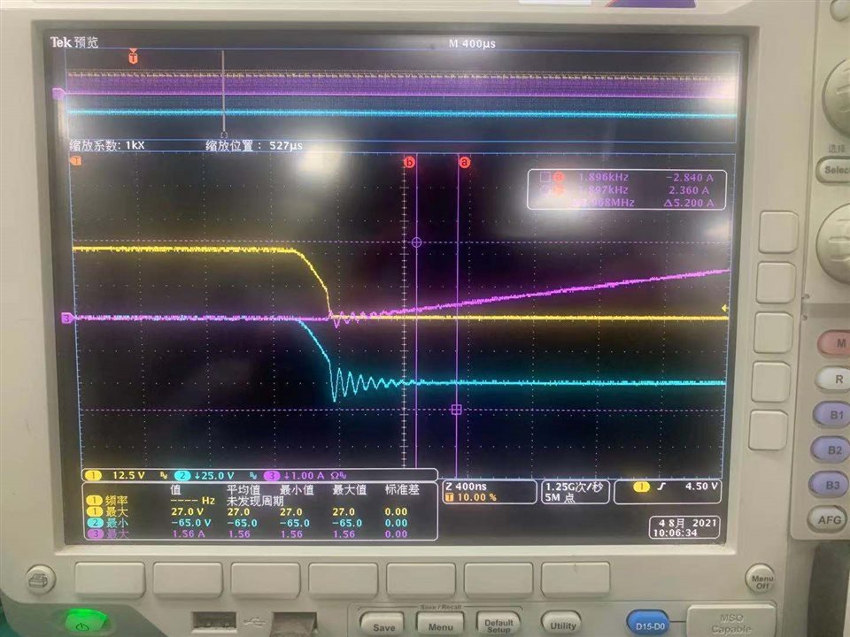
2. current overshoot at the beginning of switch conduction period (in purple)

One more question is, what is the SW turning on and off time of LM25184-Q1? Will this influence the oscillation?

Thanks,

Scarlett

  • Hi Scarlett,

    Ringing of the diode voltage is related to resonance of the secondary-referred leakage inductance with the parasitic capacitance of the diode and secondary winding. If this is of concern, please use an RC snubber across the flyback diode.

    The leading-edge switch current spike is related to current charging switch and transformer winding parasitic capacitance as the SW voltage goes to zero (it also includes current to charge the secondary parasitic capcaitances reflected to the primary).

    Both effects are expected for a flyback converter. In general, slower switching may help to reduce ringing amplitude, but this is a tradeoff with efficiency.

    Regards,

    Tim

  • Hi Tim, 

    Thanks for your reply. One more question from my side is, what's the switching on and off time of internal FET? 

    Thanks,

    Scarlett

  • Hi Scarlett,

    It depends on the operating conditions, but 10-20ns is a good estimate.

    --

    Tim

  • Hi Tim,

    Customer asks for internal MOSFET Coss value, could you please kindly provide this?

    Thanks,

    Scarlett

  • Hi Scarlett, use 200pF as an approximation.Note that the transformer and reflected diode capacitance should also be included to derive the effective SW node capacitance.

    Regards,

    Tim

  • Hi Tim,

    Thanks for your great support. We have DIN this socket in one project. Currently customer has some follow up questions, hope to get your support, thanks:

    1. Can we somehow measure the loop response? 

    I suppose FB and loop compensation is integrated in the IC we cannot break and measure the loop response as controller IC. 

    2. How do we guarantee loop is stable across the temperature/input range/output range?

    3. Customer is interested temperature compensation feature. Do we have application note explaining how to get this value? Do we have any results showing w/ and w/o thermal compensation?

    Thanks,

    Scarlett

  • Hi Scarlett,

    1. Correct, we can't measure the loop as FB is floating and is an AC node.

    2.Tthe datasheet and quickstart calculator provide min Cout for stability. We can also simulate if needed.

    3. There's an equation in the datasheet and also the quickstart calculator provides a prediction based on the diode voltage tempco.

    I'll send you an email to correspond further.

    Regards,

    Tim