This thread has been locked.
If you have a related question, please click the "Ask a related question" button in the top right corner. The newly created question will be automatically linked to this question.
Hi team,
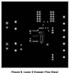
there is some confusion regarding the soldering masks of LMZM33604. The position of the pads is the same, but it seems that there is a difference in the soldering mask.
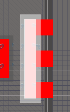
In the datasheet the blue areas seem to be metal under the pad and the soldering mask is green
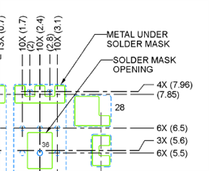
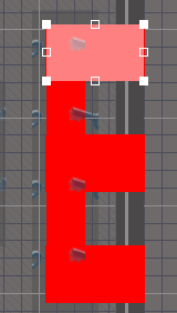
So the Altium footprint should have the same "E" shape, but like shown in the picture, the solder mask has only the shape that is purple.
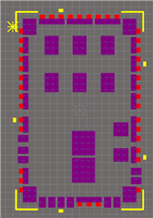
The same applies for the mask that is used for the soldering paste.
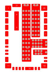
Also there are no vias in the library file, these are mentioned as optional in the DS and are realized at the EVM as well.
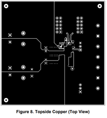
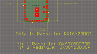
Is this related to the different padstyles shown in the following picture? Are there different geometries for the pads between which can be switched?
thanks in advance,
Jens
Hi Jens,
See below on what you can expect for the LMZM33604 footprint from TI Vault in Altium Designer.
Notice that the footprint here also doesn't have the "E-shaped" for simplicity of design.
There is currently no option to change different padstyles. I believe the Altium footprint support engineer who generated the design created it for easy of layout since it is usually recommended to pour a copper plane for those pins anyways.
Does the customer have any issue designing with this existing padstyle?
Regards,
Jimmy
Hi Jimmy,
thanks for the info.
In the meantime the developer did some investigation as well and found that the E-shaped pads of the model that can be found on ti.com are composed of a rectangular pad an additional shapes:
The mask only consider the rectangular part.
Our customer wants to avoid any issues when it comes to soldering, especially as there are 4 modules placed on the board.
Therefore a verified footprint would be necessary. Are there any reported soldering issues when using the footprint from Altium Designer?
I see you are located in Santa Clara, we can check offline if there is a chance for a customer call (time in Germany is -9h)
Regards,
Jens
Hi Jens,
I can check with the previous apps engineer who supported this to get more history on this but so far I have not heard any issues back from customers on this matter.
Looking at the LMZM33604EVM shows the topside copper and layer 2 which shows that the EVM is using the Altium Designer footprint of the LMZM33604. Notice how the EVM doesn't have any cutout areas that strictly outlines the "E-shape" of the pins.
I think having a solder copper pour plane for those "E-shape" pins should not cause any issues.
Regards,
Jimmy