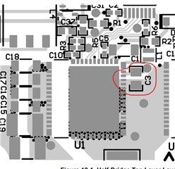
Table 6-1 describes VNEG as "Negative supply output, bypass to ground with 2.2-µF capacitor". Figure 10-1 shows the VNEG capacitor connected to source not ground. Which is correct?
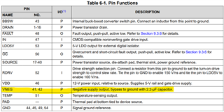
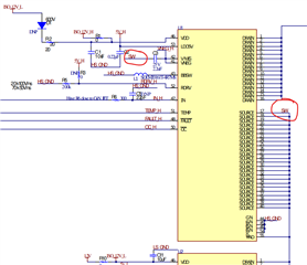
Table 6-1 describes VNEG as "Negative supply output, bypass to ground with 2.2-µF capacitor". Figure 10-1 shows the VNEG capacitor connected to source not ground. Which is correct?