Other Parts Discussed in Thread: TPS568230EVM, TPS62867, TPS568230
Hello,
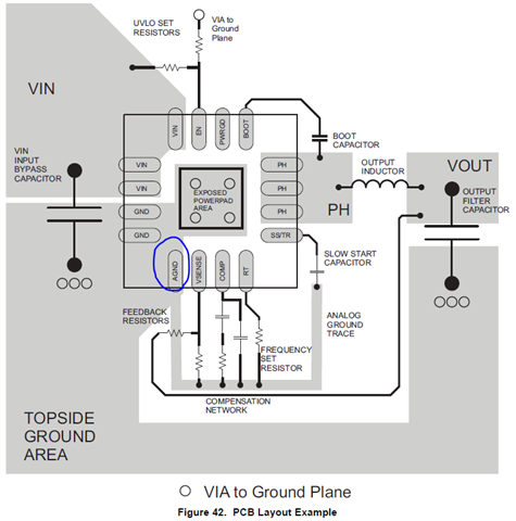
I have a question on TPS54519 layout. From my previous experience, AGND of IC should be connected on single point with GND (PGND) to prevent switching noise conducting from GND (PGND) to AGND. But TPS54519 datasheet shows GND and AGND are tied together. Is it not causing a switching noise injection problem?

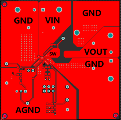
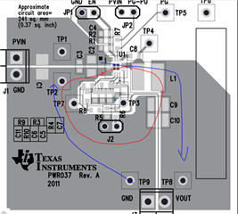
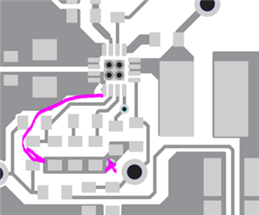
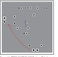
My previous knowledge is as shown below. ANGD is connected to GND plane (layer 2) thru a via.
<TPS568230EVM top layer layout>
https://www.ti.com/tool/TPS568230EVM