This thread has been locked.

If you have a related question, please click the "Ask a related question" button in the top right corner. The newly created question will be automatically linked to this question.

LMG1210: Shoot-Through Problem

Part Number: LMG1210
Other Parts Discussed in Thread: UCC27611

Greetings to all,


I try to implement H-bridge structure with GaN type mosfets. The driver I am using is LMG1210. I have added the schematic and waveforms. I will try to summarize the problem below.

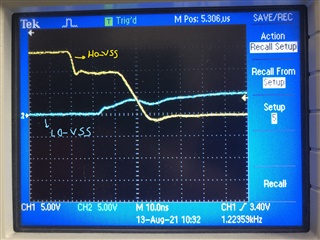
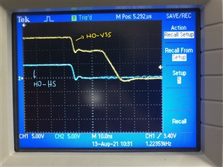
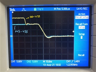
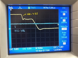
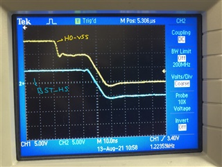
I put 47K resistor for DHL and DLH and zero ohm for both high and low side gate resistors. 47K resistor must make 12ns dead time between the falling edge of the high-side gate and the rising edge of the low-side gate. The source voltage of the high-side is decreasing until High_V at the drain, then stays there for 12ns. It looks like the high-side mosfet becomes fully off when the low-side mosfet turns on. However, it is not supposed to be like that. The high-side mosfet must be fully off, then 12ns later, the low-side mosfet must be on.


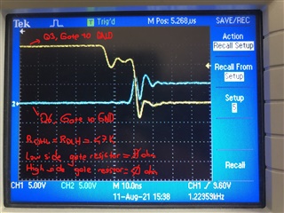
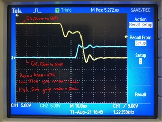
If I increase the gate resistors such as 4.7ohm at this point, even if the low-side mosfet turns on, it waits for some time to turn the high-side mosfet fully off and shoot-through occurs.


I was applying 10V for High_V for this experiment. When I give 180V, sometimes only high side mosfets, sometimes both high side and low side mosfets blow up. LMG1210 gate driver is also destroyed.


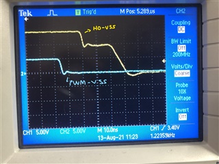
Then, I have used just a resistor instead of the coil as a load. In addition to that, I have added external freewheeling diodes on both high and low-side mosfets. Nothing changed. The waveforms are just like before. There is still shoot-through problem during falling edge of the high side.


Now, I am suspecting the LMG1210. It looks like that it is not working as it is supposed to be. I have replaced a couple of them. But the result is always the same.   


Thank you

   H_BridgeSimp.pdf

Best regards.

  • HI,

    Thank you for your question. On the plots you shared, I see the first one is the case with Rgate = 0, and the 2nd one is with low side Rgate=11 Ohm and high side Rgate = 0 Ohm. Could you please also try increasing the Rgate on the high side and share the waveform? This way the ringing on the high side gate will be reduced as well (as it did for the low side gate when you increased the gate resistor).

    If this doesn't help, then it would be good to look at more waveforms to see if there is noise on the switch node or another issue. In this case, please provide plots of PWM input, LO-Vss, HO-HS, HS-Vss, HB-HS and BST-HS all measured directly at the driver pins. 

    Also, what is the switching frequency you are using?

    Regards,

    Leslie

  • Hi Leslie,

    I have tried to increase the gate resistor of the high side. But, it didn't fix the problem.  I have included the waveforms of  PWM input, LO-Vss, HO-HS, HS-Vss, HB-HS, and BST-HS. They are all measured at the driver pins. Also, DHL=DLH=47K, High side and low side gate resistors are all 10ohm.

    Thank you.


  • Hi Kadir, 

    Please allow us until Monday to check your latest post!

    Thanks, and have a great weekend!
    DImitri

  • Hi Kadir, 

    Thank you for providing the plots. I'm reviewing them and will get back to you later today.

    Best regards,

    Leslie

  • Hi Kadir, 

    Thanks for providing the information. From the 1st and 2nd waveforms you provided (LO-Vss and HO-HS) I don't see a shoot-through event. HO-HS goes low, and about 12ns later LO-Vss goes high.

    It seems odd that HS stays high for a period of time after HO-HS goes low. I think it would be good to confirm if this is being caused by the load itself. Could you please confirm that the half bridges are switching OK with no load (without the inductor) and capture LO-VSS, HO-HS and HS-VSS again without the load? You can start testing at 100V, 150V until you get to 180V and confirm if everything works correctly. 

    Also, the diode you are using is rated for 200V and your bus voltage is 180V which leaves very little margin. I recommend changing the diode for one that is rated 2x the bus voltage to have a higher margin for transients. 

    Best regards,

    Leslie

  • Hi Leslie,

    Thank you for your recommendation about the diode. I will consider that.

    On the other hand, I had used purely resistive load while I was getting the last waveforms as I suspected it. 

    I have removed the load resistor for you though. All the waveforms are still exactly the same as the last waveforms I posted. So, it looks like the problem is independent of load.  

    Thank you.

    Best regards,

  • Hi Kadir,

    Thanks for checking that. The very first plots you shared (where you measured directly at the gate of the low side FET and the high side FET) show overshoot/undershoot that exceeds the abs max ratings of the transformers you are using. However, I suspect this might just be added parasitics from the probing method. Could you please confirm how you connected the oscilloscope probes to the pins? We recommend using tip and barrel method directly at the pin to avoid incorrect measurements due to the probes.

    What is the switching frequency you are using?

    Regards,

    Leslie

  • Hi Leslie,

    All the plots so far have been measured with the tip and barrel method directly at the pin.  

    My H-bridge structure is actually more complicated. The very first plots I shared belong to this complex H-bridge structure. I have simplified that for you in case you don't confuse and focus on the problem. The plots in my second post belong to that simplified H-bridge structure that I shared with you.

    The switching frequency I use was very slow during the tests. It was 2.5kHz with 4% duty cycle. 

    I also want to remind you that the voltage I am working on is 10V for the test. When I increase it especially above 100V, GaN fets, and sometimes drivers blow up. 

    Thank you

    Regards,

  • Hi Kadir,

    Let me review this case with our internal team and I'll get back to you tomorrow. In the mean time:

    • Does anything fail at 10V, or do the failures only happen when you go to higher voltage?
    • With your simplified H-bridge structure, are you still seeing GaN FETs blow up when increasing the voltage to >100V?
    • Is there a reason why you are using different FET part numbers on the high side compared the the low side of each half bridge?

    The reason why I was concerned with the very first plots you shared is because the FET's abs max specs are being exceeded. Therefore, I'm trying to understand if these specs are still being exceeded when measuring at the FET gate pin with the simplified H-bridge structure. 

    Best regards,

    Leslie

  • Hi Kadir, 

    Are the FETs still getting damaged even after removing the load?

    If you haven't done this already, please find out if the issue follows a specific device or a specific board. To check if the issue is on a specific board, you can test a known good driver on a new board and on the board you are currently using to capture the plots. You might have already done this since earlier but I wanted to confirm is not a board specific issue or IC specific issue. 

    Regards,

    Leslie

  • Hi Leslie,

    Sorry for the late reply.

    • Does anything fail at 10V, or do the failures only happen when you go to a higher voltage? 

                It doesn't fail at 10V. It fails at higher voltages.

    • With your simplified H-bridge structure, are you still seeing GaN FETs blow up when increasing the voltage to >100V?

                 Yes, I do.

    • Is there a reason why you are using different FET part numbers on the high side compared to the low side of each half-bridge?

                Yes, there is. I need a GaN Fet that has a higher current rate at the low-side for the complex H-bridge. 

    • Are the FETs still getting damaged even after removing the load?

                 Yes, they are still getting damaged.

    • If you haven't done this already, please find out if the issue follows a specific device or a specific board. 

                I have checked the system with many GaN FET drivers with three different boards. I got the same problem every time.

    In the meantime, I used UCC27611 for high and low sides instead of LMG1210. The shoot-through doesn't appear with UCC27611.
    But I got some oscillations because the drivers were assembled a little far from the GaN FETs with fairly long wires. I am suspecting that something disturbs the integrated high and low side structure of LMG1210 and causes the shoot-through.

    Thank you.

    Regards

  • Hi Kadir, 

    I'm sorry to hear you are still having issues and I'm glad you have a temporary replacement part. 

    I followed up with our internal team regarding the fact that the HS-Vss voltage is staying high until the low side FET is turned on. Here is the explanation for this happening: 

    During the dead time both HO (w.r.t. HS) and LO (w.r.t. Vss) are pulled low, and during this time the switch node (HS) should be in a high-impedance (Hi-Z) state. Since there is no load connected to the switch node, there is no current going out of it when it transitions to Hi-Z. Therefore, the switch node will stay static, since there is nothing to discharge the output capacitance of the high-side and low-side FETs, and the switch node (HS) voltage will stay high until the low side FET turns on.

    From the waveforms you shared, the waveform shows plenty of time between HO-HS going low and LO-Vss pulling high. 

    The next step I would recommend is to capture the waveforms (still without a load) gradually increasing the bus voltage. Seems like the issue you are having cannot be seen at 10V, but as you increase the voltage you might be able to identify if there is ringing or overshoot/undershoot that is occurring that exceed the FETs abs max rating at higher Vbus voltage, which could lead to FETs damage (and driver damage as a consequence).

    Best regards,

    Leslie

  • I also don't see any evidence of actual shoot through in the waveforms. When there is no (or very little) load, the HS voltage is expected to maintain its level during the dead time. That's exactly what's happening in all the attached waveforms.

  • Mike,

    Thanks for your inputs. That's correct. The next step I would recommend is to capture the waveforms (still without a load) gradually increasing the bus voltage. Seems like the issue you are having cannot be seen at 10V, but as you increase the voltage you might be able to identify if there is ringing or overshoot/undershoot that is occurring that exceed the FETs abs max rating at higher Vbus voltage, which could lead to FETs damage (and driver damage as a consequence).

    Regards,

    Leslie