This thread has been locked.

If you have a related question, please click the "Ask a related question" button in the top right corner. The newly created question will be automatically linked to this question.

TPS568230EVM: Layout for AGND and GND

Part Number: TPS568230EVM
Other Parts Discussed in Thread: TPS568230, TPS54519

Hello,

I have a question on TPS568230EVM layout.

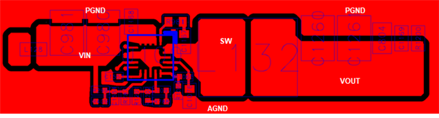
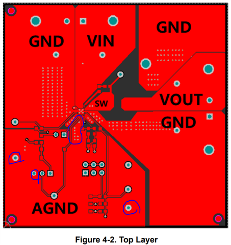
When I look at the top layer :

-  GND plane (pin 7, 8, 18) and AGND plane (pin 13) are separated, and should be connected in a single point

-  AGND pin should not connect to thermal pad

-  Those layout practice is for preventing switching noise conducting from GND to AGND 

But here comes my questions : 

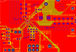
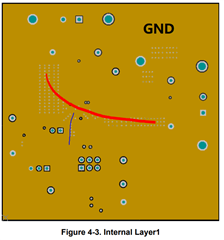
 AGND and GND look completely separated in the top layer and connected in the layer 2  (GND plane) thru many vias. (I mark with blue color on the image above) I wonder how this helps to decouple the noise from GND to AGND.

To my knowledge, AGND and GND are separated at the top layer just like the EVM, and connected thru a short trace of thru a 0ohm resistor, so that the noise is hard to be injected to AGND plane. But it looks the connection to GND plane thru many vias cannot effectively isolate AGND from GND switching noise. Could you help me to understand the recommendation layout here? 

  • Hi Ella,

    Yes, that's seldom to use on the EVM design since EVM has enough area for the direct connection between AGND and PGND on the same layer of IC. But that's some connection method that many customer would always apply. Single point connection with 0ohm or short trace is great, but the direct connection will cause large routing area. For some customer's application with small solution size requirement, it's hard to complete that. But customer always have large PGND plane in internal layer for their board design, so it's easier to achieve small solution size with vias.

    Basically, the single point connection is to block the high frequency noise from PGND to AGND. With the vias parasitic inductance, that could also help to block high frequency noise.

    Thanks,

    Andrew

  • Andrew,

    Your comment is so clear! Thank you for that.

    I have one additional question. EVM shows AGND pin (pin 13) is not connected to thermal pad. But customer connect this pin to thermal pad, and AGND pin is not directly connected to analog circuits' GND, such as the voltage set point divider, EN resistor, SS capacitor, MODE resistor. 

    Do you expect any critical issue here? Datasheet does not describe about AGND pin connection to thermal pad. I believe following the EVM layout would be safe for noise but customer requests for double-check as they want to stay on their current layout.

    * both images are same layout with the different viewer.

  • Hi Ella,

    I think we have talked through email.

    According to the upper image, customer layout, AGND is connected to thermal pad GND and Pin 7&8&18. It means AGND is directly connect to GND, power ground. The power ground bounce during switching will directly conduct to AGND.

    AGND is not only the analog ground of EN, SS or MODE, it is also the ground of internal logic circuit. 

    Thanks,

    Lishuang

  • Regarding the TPS568230


    AGND is connected to the GND(labeled PGND top layer ) on 2nd layer  through the vias.

    The AGND has multiple vias connecting to  AGND to PGND. 

    The high currents are not flowing in lower left of the board on the top and 2nd layer.   The current is flowing on the red mark and the blue is the agnd connect.    An improvement to the board could be having a cut in the 2nd layer plane to insure current will not flow along the agnd vias.

    For the TPS568230, the current path is under the device, it is best to connect AGND to PGND away from device.  TPS568230 is higher current and narrower pin pitch than TPS54519


    .


  • Hi David,

    Thank you for your comments and all details. Could you kindly help me to understand what your comment below means? I believe it's the case applied also for TPS54519. Can it be a reason why TPS568230 does not recommend to connect AGND to power pad unlike TPS54519? 

    For the TPS568230, the current path is under the device, it is best to connect AGND to PGND away from device.
  • On the TPS56830, the power currents are flowing on the top and bottom side of the board and through the vias. 

    Currently, the way the board is laid out.  Connecting the AGND to PGND with vias slightly away from the device. 

    The AGND vias connect to the PGND plane on the other layers (lower left).   If AGND connected to PGND under device, it is possible some of the top layer power current would flow trough the AGND vias, cuasing different voltages on the grounds on the sensitive analog components.     The way to ensure current does not flow on top layer to the lower left of board is to omit the trace from agnd to thermal pad on the top. 

    So there probably another way to layout out this board. 

    If the board was redesigned.  I would recommend that the schematic have an AGND and GND symbols and use a net tie  (or zero ohm resistor) to tie AGND to PGND.    The zero ohm resistor allows nets to be isolated when pouring copper.  This would prevent AGND vias from connecting to PGND then I would connect the AGND with a via to PGND on second layer with a via near the agnd pin or i would connect AGND to thermal pad on top.   using the AGND net, allows the sensitive analog component to connect the PGND in exactly one location.