This thread has been locked.

If you have a related question, please click the "Ask a related question" button in the top right corner. The newly created question will be automatically linked to this question.

TPS6594-Q1: PMIC Not working - TPS65941212RWERQ1 and TPS65941111RWERQ1

Part Number: TPS6594-Q1

Hi

The customer does not operate PMIC during the board test with PDN-0BX.

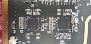
Please review if there is a problem with the schematic.

Delete Schematic.

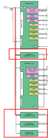
1. TPS65941212RWERQ1
VOUT_LDOVINT : 1.8V output.
VOUT_LDORTC: 1.8 V output.
Other BUCK and LDO: Not output.
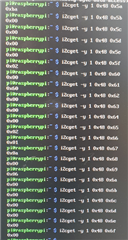
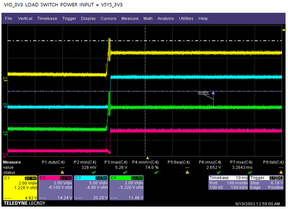
Note: As shown in the attached screenshot, GPIO3 (EN_MCU3V3_LDSW) moves for about 1 second and then falls to LOW.

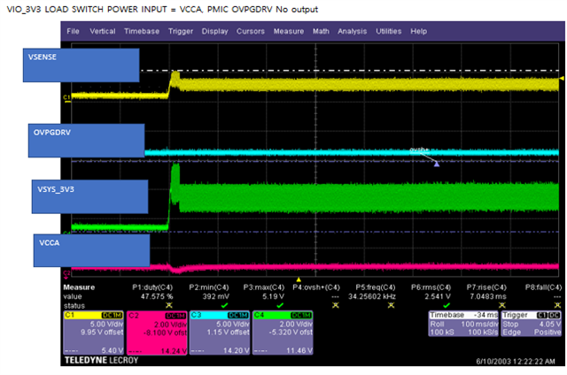
TPS65941212RWERQ1 RSTOUT Pin (GPIO11) waveform.


2. TPS65941111RWERQ1
VOUT_LDOVINT : 1.8V output.
VOUT_LDORTC: 1.8 V output.
Other BUCK and LDO: Not output.

  • Hi, Cho,

      Please make correction first: the FB-B3 pin of TPS65941212RWERQ1 should be connected to VDD_DDR_1V1.

    Thanks!

    Phil

  • Hi Phil,

    I'm sorry. It's a schematic attached error.

    The FB-B3 pin is connected to VDD_DDR_1V1. Update the latest schematic.

    i-ecu_rev-c-1_2021.pdf

    After PMIC is powered on, it seems to be a problem in the i2c communication stage between PMICs.

    In the traditional Pdn-0ax, the output is coming out regardless of output load and voltage/current sense.

    Attaching the 0bx chipset to the functioning Rev_B-3 Board (board for pdn-0ax, remove Load) does not progress in the i2c operation phase between the pmics.

    PMIC A – B Swap tests produce the same I2C waveform.

    20210822_iECU PMIC check_EN.xlsx

    Could it be the issue of Nvram?

  • Hi, Cho,

      From the schematics and Excel file you attached; it's not about the i2c communication; it's about SPMI between PMIC A – B. They can't be swapped; they don't work at all after swapped although the same waveform could be seen.

      Their 30 and 31 pins are for I2C communication with the processor as showing by screenshot below. Please read PMIC-A (I2C address 0x48) interrupt registers from address 0x5A to 0x6C to check the reasons of not power up properly. 


    Thanks!

    Phil

  • Hello, Phill.

    "I2C" operation between PMIC means  "SPMI" interface. (LEOA_SCLK & LEOA_SDATA using GPIO5 and GPIO6)

    Below is the same symptom and adding some questions.

    1. PMIC is supplied the input power (3.3V) without input over-voltage fault status.

    2. internal two 1.8V LDO of each PMIC works fine.

    3. Next step (I think) PMIC-A check something with PMIC-B, but after communication, PMICs change the status to fault condition.

    in this time, PMIC try to enable some GPIO (MCUIO3V3) and output power very short time (as excel sheet).

    Question

    1. Would you please what information checked initial SPMI communication between two PMIC when initial powered on? 

    2. After enable the GPIO3 (MCUIO_3V3), Which can make change the PMIC status to fault condition?

    3. When first time (As per NVRAM, without CPU I2C communication), PDN-0Bx PMIC sense the output voltage or current?

    Thanks.

    S.H

  • Hi S.H,

     A1: All fault conditions that cause interrupt should be checked with both PMIC-A&-B registers address from 0x5A to 0x6C.

    A2: GPIO3 is used to enable MCUIO_3V3 power rail; if the rail has issue, it cause a fault condition. 

    A3: Yes; even without CPU I2C communication, PDN-0Bx PMIC has sense to its power rails output voltage or current.

    Thanks!

    Phil

  • Hi Phil.

    1) Please review the register value. 

    2) Please review the schematic, Mr,Cho requested.


    20210824_iECU PMIC waveform review.xlsx

    3) I reviewed waveforms. PMIC stopped after 2nd power up stage (active sequence is ~ 1700us) as attached file..

    I think the Buck FB_B3  DDR1V1 monitor is working 4th stage, but in my board condition is stopped 2nd stage, it is not starting monitoring. Is that right?  (please see the attached file.)

    Best regards.

    S.H

  • Hi S.H,

     1) From register value, it shows LDO4 has an issue. Please try to reduce the cap on LDO4 output; higher cap value may cause LDO ramp up too slow to cause the interrupts below.

    2) Schematics has no big issue. It's better to tie GPIO9 of PMIC-1 and GPIO1/7/8 of PMIC-2 high or low since they're inputs without any internal PU or PD.

    3) No; it's not the issue of power down. 

    Thanks!

    Phil

  • Hi, Phil.

    Thank you for feedback.

    I removed some capacitors related LDO4, issue is cleared !

    And two more questions.

    Q1) What is maximum allowable capacitance for LDO4?


    And I found another issue related VSYS_SENSE.

    When powering on the unit, frequently PMIC VSYS_SENSE failure observed as below screenshot. (Sometimes automatically recovered, but sometimes hanged.)


    And I try to change the power source of load switch for VDD_IO_3V3, VCCA to VSYS_3V3,  issue is disappeared. (even if Vsense peak voltage is higher.)


    In application note (slvuc32) 5page block diagram, load switches are connected VCCA source.

    Q2> Could please advise the correct power source connection for VDD_IO_3V3 load switch? 

    Q3> If the power source connection is correct (VCCA), what can be impact VSYS_SENSE ?

    Thanks!

    S.H

  • Hi S.H,

    A1: Please see datasheet screenshot below:

    A2: VCCA.

    A3: VSYS_SENSE failure is caused by the VSYS_3V3; Overshot on VSYS_3V3 should be fixed. 

    Thanks!

    Phil