Dear Sir/Madam,
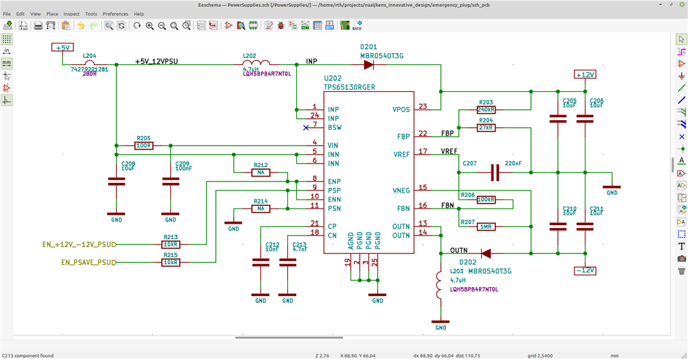
I designed a symmetric +/-12V supply based on the datasheet of the TPS65130 controller for useage is a EV charger related application.
The schematic is shown below (i have also added a 7.5pF NP0 capacitor on top of R207 on the PCB, so in parallel with R207), since this cap is prescribed by the datasheet.
- The 10uF capacitors on the output are 10uF 1206 35V X7R capacitors (40% capacity derating at 12VDC)
- The +12V and -12V supply are both running in NON-powersave mode.

After applying load steps: 12mA to 36mA on the -12V supply (done by switching load resistors), I noticed that there are quite some oscillations in the -12V regulation. See figure below:

The yellow signal is the measured voltage over a 1Ohm shunt resistor which is in series with a 500Ohm load resistor. (This load resistor is switched between +12V and -12V.)
The -12V output contains a 1kOhm resistor which is permanently between -12V and GND (so 12mA load current).
The blue signal represents the AC coupled -12V voltage.
I do not have loop response equipment available at the moment, but normally the oscillation after a load step response indicates a phase margin smaller than 40 degrees. Which is in general not desired in power converters.
I have verified the following:
- Is the Input voltage stable during load step? --> yes fixed +5.0V with < 20mV ripple.
- Are there additional capacitors on the -12V rail on the PCB with significant capacity? --> no, less than 1uF in total
- I placed an additional 10uF X7R cap close to the INN pin of the TPS65130 (allthough C208 was already close) --> no difference.
- At the end I found out that increase the 7.5pF feedback capacitor to 27pF results in a much better load step response, see figure below:

As shown in the scope image, the oscillation has disappeared.
Do you think that this is a good solution? In case I just follow the guidelines of the datasheet (and reference design) I am not able to get rid of the voltage oscillation as a result of the loadstep.
How can I verify loop stability by design (simulation) with this TPS65130? I could not find any tool or simulation model on the TI website by which this can be simulated.
I would like to thank you in advance.
Kind Regards,
Roel ten Have
ps.
- the load step response of the +12V is already good with the prescribed feedback resistors/capacitors. (no oscillations)
- the load step response of 12mA to 48mA on the -12V was even worse, see figure below as an indication:


