This thread has been locked.

If you have a related question, please click the "Ask a related question" button in the top right corner. The newly created question will be automatically linked to this question.

UCC3895: slope compensation circuit

Part Number: UCC3895
Other Parts Discussed in Thread: UCC28951, UCC28950, UCC2895

Hello TI.
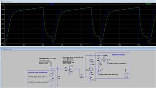
I am stuck with my DC-DC converter based on UCC3895. Basically, my circuit is almost the same as in the datasheet. The problem is that under light load (~2W) converter is unstable (crackle noise, rapid duty cycle changes). @50W load everything fine.
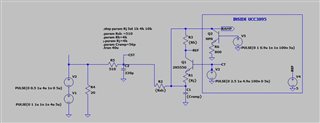
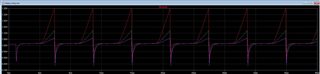
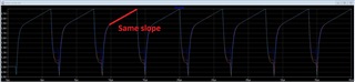
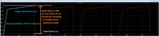
I have been told that such a problem can occur due to the poor slope compensation circuit. Here as I understand this phenomenon: As under light load there is almost no CS signal converter works only using ramp, generated by the slope compensation circuitry. This ramp looks quite poor because it doesn't rump up from zero and has DC bias which may cause unstable operation when EAOUT voltage is near this DC bias of the rump. Also, no-load comp kicks in.
Can you confirm that it makes sense or am I wrong with this explanation?
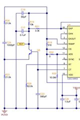
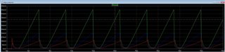
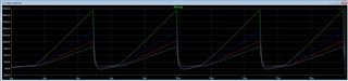
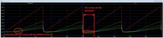
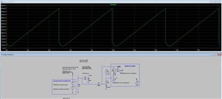
Modeled slope comp:

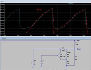
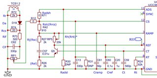
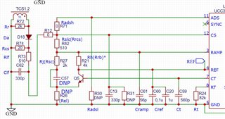
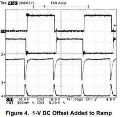
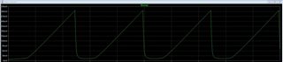
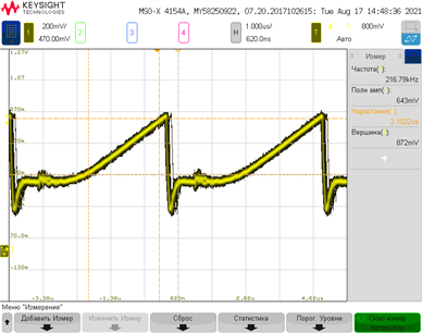
This is measured voltage on ramp pin when only PWM controller enabled. No HV at the input.

Also, I have some questions about slope compensation circuitry in datasheet.
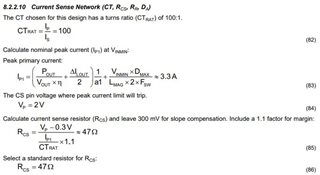
1) P.39 of the DS «The 10-kΩ resistor RRB provides approximately 250-mV offset bias. The value of this resistor may be adjusted up or down to alter the point at which the internal no load comparator trips»
 So how exactly can it alter the point at which the no-load comparator trips if the no-load comparator is directly connected to the EAOUT pin and 0.5/0.6 reference?
2) Formula #118 at p.38 it probably should have Msum instead of Mmag at the denominator?
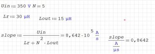
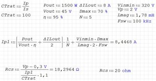
3) What amplitude value and shape should have proper slope compensation to ensure robust operation within full load range 0A up to Imax? How can I estimate Rsum value?
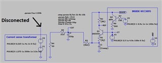
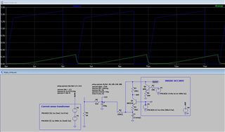
Schematic included.

Schematic_PSFB_2021-08-26.pdf

  • Hello

    I reviewed your schematic and PR1 does not look correct.  That would only be needed if you sized the current sense resistor R74 incorrectly.  So I would remove that resistor and resize R74 correctly.

    Also you slope compensation circuit is not setup correctly.  Please refer to figure 18 in the data sheet for the correct connections and compare them to yours.

    The UCC28951 evaluation module EVM also has an example of how this slope compensation should be setup in figure 1.  https://www.ti.com/lit/ug/sluu109b/sluu109b.pdf

    The way Q5 is setup it is not providing any slope compensation to CS.  The Q5 emitter should be tied to a resistor that goes to the CT pin.  This resistor will form a voltage divider with a resistor that goes to the CS pin.  I believe in your circuit C57 should be terminated to ground.  R26 should be connected from the emitter of Q5 and not C57,  R26 should not be connected to ground but to the CS pin. R42 and the ramp pin are not connected correctly.  Refer to the data sheet and EVM example for correct circuit setup.

    The RAMP is only supposed to discharge the CS pin to ground.  It should be a low impendence.  

    Regards,

    Mike

  • Hello, Mike!

    Thank you for your attention to my question! Hope my schematic didn’t take too much of your time. Please  ignore RP5 for now, I have put it there by mistake. Now it is in the upper 5k limit, and it is only providing little load at the CS signal. A am not trimming it.

    I can clearly see discrepancies in my schematic with the one on figure 18 of the DS and on figure 1 in the EVM document. (fig.1 EVM and fig.18 DS are the same indeed) The reason for this discrepancy is that I have referred to figure 24 in the datasheet of UC3895 when designing my slope comp circuit. The schematic at that figure is not the same as at figure 18. The design procedure is also referring more to figure 24 rather than figure 18. Can you confirm that figure 24 provides incorrect schematic?
    Also I am little bit confused by this:
    The Q5 emitter should be tied to a resistor that goes to the CT pin.

    I am sorry, but it there some kind of typo? Since no schematic has a resistor that goes to the CT pin from emitter... Maybe you meant RAMP pin, not CT?

    Regards,
    Vasiliy 

  • Hello

    Q5 is on your schematic you attached.  I double checked it.

    The Ramp pin actually does not apply a PWM ramp.  It is supposed to discharge the soft start capacitor.  The data sheet suggests using an NPN transistor to buffer the CT signal.  So I thought that is why you added Q5 to the circuit.

    Your present circuit does not have slope compensation.  You should be able to create this off the CT with an NPN transistor and resistor divider to the CS pin and the current sense resistor.  I would think about 200 to 300 mV would do it.

    Regards.

  • Sir, please apologize if my question was unclear. Please give me one more chance to clarify my question.

    Look at the schematic at p.40 (Figure 24) in the data sheet of the ucc3895. Here it is:

    Here is my schematic:

    Q5 is NPN type transistor in both schematics. Emitter goes through  R23-21k (R26-2k in my schematic) to the ground. Also the emitter of Q5 goes through  C24 (C57 in my schematic) and R26 (R27 in my schematic) to the RAMP pin. Collector of Q5 goes to REF in both schematics and through R19 (RP5 in my schematic) to the RAMP pin. Base of Q5 goes to the CT pin in both schematics.

    I simply copied this Figure 24 in my schematic so they are almost te same. The only difference in some values. Do you agree with this or am I missing something?

    Your present circuit does not have slope compensation.

    If these schematics are the same,  the circuit at p.40 (Figure 24) in the data sheet of the ucc3895 does not have slope compensation either. So that question that I am asking: Does circuit at p.40 (Figure 24) in the data sheet of the ucc3895 is incorrect?

    So the only correct schematic in the data sheet I should use is fig.18 p.22?

    Regards,


    Vasiliy 

  • Hello,

    I don't believe figure 24 in the data sheet is not correct.  This is probably why your CS signal has a DC offset. 

    In most circuits for slope compensation you only require an NPN transistor as buffer to the CT pin.  Then you divide this signal down with a resistor divider to the CS pin. Not sure what they were trying to accomplish in figure 24.  

    Figure 18, Q1, Rj and Rslc is the circuitry that should be added to provide slope compensation.  It looks like they added CRAMP for high frequency filtering.  Not sure why they had to add resistor RH.

    Regards.

  • Hello,

    I found out what RH was for.  The following application note written by Steve Mappus explains why it was needed. 

    https://www.ti.com/lit/an/slua275/slua275.pdf

    Regards,

  • Hello, Mike!

    I changed my schematic according to figure 18 in the datasheet. Here it is:

    I also build a model of this slope compensation circuit using LTspice and it fit real data:

    No signal has been applied from CST. Rj=1k red waveform, Rj=4k - blue one, Rj=10k - pink. Real waveforms look the same.

    This from appnote you linked me. Same DC-bias in my case.

    But I am missing some crucial point – how exactly does this circuit compensating? I simulated this schematic with 3 different values of Rj 1k 4k and 10k and it gave me exactly same slope in all cases as soon as i connect signal from the CST!

    Here is my "ideal" signal from the CST (tdead = 1u)

    Here is RAMP output when signal from CST has been applied (with 3 values of Rj look at the colors):

    What did I miss?

    Here it the Link to the google drive with my LTspice file.

    Regards,
    Vasiliy 

  • Hello,

    The circuit from the app note just shows why the offset resistor from VREF to RAMP is needed.  It was to remove the asymmetrical pulse.

    Not sure what the component values are the author did not include them.

    The CT oscillator ramp is supposed to vary from 2.35 V down to 0.2 V. This will be dropped down to 1.4 V with the NPN transistor.  This agrees with your ramp waveform.  The RAMP waveform also shows the DC offset of 1V.  So it looks like you have copied the circuit.

    I have experience designing with the UCC28950 and UCC28951 these devices have internal slope compensation and have not needed this offset.

    When I read this app note it looks like at light loads the controller was trying to demand a minimum duty cycle and the offset was added to limit the duty cycle.  To get 0% duty cycle the C and D pulses will be phase shifted and will look asymmetrical.

    Could you try removing the DC offset to this circuit by removing R21 to see what your RAMP looks like.  I think it will be closer to what you expect.  Also if you need an offset at the ramp pin to get rid of the asymmetrical pulses at light loads I would start by adding a 100 mV.  I think 1 V is way too much.

    Regards,

    Mike

  • Hello, Mike!


    In fact, even 800mV is not enough to eliminate asymmetrical operation. At least for my particular IC. I tested on a bench prototype. 1V offset is fine, the duty cycle is symmetrical all the time.

    I am a little bit confused about how the signal should look  at the ramp when compensatedThere should be a signal ramping up to some value with certain dv/dt that I set by Rj. Isn’t it? So as you said I removed the DC-biasing resistor and indeed, the Rj value slightly changes slope, but only when no signal from CST is connected...

    When I connect my CST signal, the change in slope just vanishes. Something wrong with my values?


    Regards,
    Vasiliy

  • Hello,

    When you removed the DC offset the ramp signal should look similar to what you have.  It looks like you are adding 900 mV of PWM that is quite it a bit.  The ramp you add should be about 200 to 300 mV.  So that is quite a bit. I would adjust this down to 300 mV.  It is generally half the down slope of the reflected output ripple current seen by the CT.

    The shape of your CT signal and added ramp looks correct.   Do you know what the voltage across R74 is supposed to look like without the slope compensation added?  I am thinking that your slope compensation is so excessive you can see the affects of the output inductor ripple current, you are just seeing the added slope comp.

    Try adjusting your slope compensation down to 300 mV to see if the behavior changes.  You may also want to study the transformer primary current to get an idea of what the voltage across R74 should look like and the appropriate amount of slope compensation you need.

    Regards,

  • Yes sir. I think I am understanding how the voltage across R74 should look. Here is my model of this waveform. First slope caused by shim inductor and determined as dI/dt=Uin/Lr. Second slope is determined by Lout as dI/dt=Uin/(Lr+n^2*Lout). As a first order approximation it should work. Correct me if I am wrong. I also scaled this amplitude (assuming full load) according to the formula 85 at p.33 in the datasheet. Here is what I got:

    Let’s first look at the ramp voltage if the signal from CST isn’t connected to the circuit. (Similar to no HV at the converter input). Slope compensation is around 300 mV, as you recommended.


    Now I have connected the signal from CST to the rest of the circuit and… Yes, the waveform did change, but the slope is the same. Moreover, slope is the same at all values of Rj. Could you please explain what I am missing

    Sorry, It must be something simple and stupid, but I am really stuck with this problem...

    P.S. I hope I don't bother you too much with my problems...

    Regards,
    Vasiliy

  • Hello,

    What should be the dv/dt across the current sense resistor (R4) based on the reflected output inductor current across the transformer and the magnetizing current?

    The ramp voltage that you are seeing on your last waveform looks like it is all slope compensation.  This could mean that change voltage across R4 caused by the reflected output current and transformer magnetizing inductance is a lot smaller than the slope compensation.

    Change in VR4 = ((Change in ILout)*(Np/Ns) + Change in ILmag)*R4 << Vslope Comp  = 330 mV.

    The CS and slope compensation waveforms you sent look much better than what you started with.  Did this resolve your original issue of hiccup mode at light loads?

    Regards,

  • What should be the dv/dt across the current sense resistor (R4) based on the reflected output inductor current across the transformer and the magnetizing current?

    It is should be 0,86 V/us. Here is my calculations.

    The ramp voltage that you are seeing on your last waveform looks like it is all slope compensation.  This could mean that change voltage across R4 caused by the reflected output current and transformer magnetizing inductance is a lot smaller than the slope compensation.

    Yes, but isn't the slope of this ramp voltage dependent on Rj value? Shouldn't I see a different slope at different values of Rj? Or am I missing something?Because in my case the slope is the same all the time. And it doesn't depend on Rj value. Something wrong with the circuit? How can I ensure that the circuit is working and how can I see the compensated slope?

    The CS and slope compensation waveforms you sent look much better than what you started with.  Did this resolve your original issue of hiccup mode at light loads?

    In fact it has become even worse. Instability occurs even at higher load ranges. But I tried only with Rh=2k to ensure Ramp biased above 1V. If it isn't biased, asymmetrical operation could cause saturation of the transformer and destroy the transistors.

    Regards,
    Vasiliy

  • I have some doubts that I understand how this should work. Is it correct that compensation voltage is adding to the current signal? And this sum forms a compensated CS signal fedded to the ramp pin.
    Here is compensation voltage (values for Rj=6k,10k,14k,18k) forming by Q5 at the ramp pin (no current signal)

    This voltage will be added to the signal from current sensor. Correct?
    So, let's assume our current sensor signal (blue waveform) duration is 2us.

    (Green signal is compensation voltage and red is CT internal ramp)
    How then compensation voltage can be added to this signal if compensation voltage only starts ramping after 1.5us? Does this mean that slope compensating won’t work with current signals less than 1.5us or I am understanding it incorrectly?

  • Have you account for your current sense transformer turns ratio?

    IR4/TRANSFORMER = Nct1/Nct2

  • Hello,

    I looked at your simulated waveforms and see a flat spot that you show on the RAMP pin.  The CT signal varies from 0.2 V to 2.35V.  When the CT voltage is below 0.6 V to 0.7V Q1 will not be forwarded biased.  You are correct that there will not be a ramp generated if there is not enough voltage to pass current drain to source.

    Similar slope compensation circuit with a NPN transistor and resistor divider similar to the one you are evaluating have been used for many years for slope compensation.   I believe these design may have had similar issues if the CT voltage varied down to ground like the UCC2895.

    The slope compensation was originally added to remove sub harmonic oscillations due to transients.  Later it was discovered that some PWM ramp at light loads to give a PWM signal because the CS signal was not large enough.  This presented the converter from bursting and producing audible noise.

    If you find that the flat spot in the slope compensation presents and issue you could add a buffer to the CT pin to resistor R1.  This would remove the flat spot.

    Regards,

  • Thank you for this explanation, Mike! It became clearer to me now.
    I also remembered that there is no need for slope compensation if the duty cycle is < 50% so that flat region should be ok for higher load range.
    But I still don’t know if it is the culprit of bursting and producing audible noise at low loads.

    If you find that the flat spot in the slope compensation presents and issue you could add a buffer to the CT pin to resistor R1.  This would remove the flat spot.

    Could you advise a circuit that will be a proper choice for compensating at low loads? Is there any appnotes covering this method or something more detailed? Calculating examples for UCC3895?

    I have accounted for my current sense transformer turns ratio. I used formula 85 at p.33 in the UCC3895 datasheet to calculate my values.

    This formula is based on the maximum current signal of 2V peak – 0.3V slope compensation. In my simulation I feed 1.5 V peak current signal to the compensation circuit. And the circuit can’t add 0.3V to 1.5V for some reason…

    Here is what I am talking about: green waveform ~300 mV pk. Blue is 1.5V pk. Current transformer is disconnected. When I connect it to the circuit it should add 0.3V+1.5V and it will compensate.

    But when I connect the current sensing transformer to the circuit, it doesn't add those 0.3V to the 1.5. It is just 1.5Vpk so it isn't compensated. What's the reason?

    Regards,
    Vasiliy

  • Hello Vasiliy,

    I am looking at this circuit for the UCC2895 and I think your simulations might be correct. 

    I reviewed the application circuit and NPN circuit is supposed to be a buffer.  The CT ramp varies from 2.35 to 0.2V.  So part of the issues is that  when the ramp is below 0.6 V there is nothing added.

    The second issue is when the CS signal can become large enough so NPN transistors base emitter junction is not biased.  That is probably why you are not seeing the slope comp in your simulation.

    I have experience designing with the UCC28950 that has internal slope compensation.  I am going to discuss this with my colleges to see if we are missing something.

    Regards,

    Mike

  • Hello,

    I gave this some thought last week and I don't believe this slope compensation circuit is that good.  I would recommend using a high instead. divider off of CT instead.

    1. Remove Q1 and Connect R1 to CT.

    2. Disconnect R2 from CST and connect it directly to R4 (Current Sense).

    3. R5 and C2 should be connected to CS of the UC2895, OCP protection

    3. Set Rj = 909k

    4. Set R2 = 110k

    5. Set C1 to 1.5 pF, this will give you a low pass filter at the ramp pin of 1.086MHz

    6. This circuit should give you 232 mV of slope compensation.

    This may slightly affect your switching frequency of the UCC2895.  However it should not be much.

    However, if so just slightly decrease your RT resistor so it runs at a higher switching frequency.

    Regards,

  • Hello Mike!I really appreciate your help! I think I understand now, how this circuit should look like. So the next step is to try it on a bench to see if it will resolve hiccup issue.I also made an LTspice model, please see attached picture.

    Is this circuit correct now? BTW is there a formula to estimate added slope? How can I calculate Rj for different compensation conditions?And let me ask a little bit off topic. There are few mistakes in the UCC3895 datasheet. I can list it here, but will you correct the datasheet according to this? Or it will be useless and the datasheet will not be corrected?

    Regards,

    Vasiliy

  • Hello Vasiliy,

    The schematic looks correct.  If you need to adjust the slope compensation it is resistor divider.  You can do this from the oscillator ramp amplitude.

    The following equation will do it.

    Vramp = (2.35V-0.2V)*(Rslc+R4)/(Rslc+R4+Rj)

    You will be much happier with the results.

    Regards,

    Mike

  • Thank you Mike! I think we discussed enough for now. Will try to implement this circuit on a bench.

  • Hello,

    I believe this should work for application.  I was glad that I could help.

    Mike