Because of the holidays, TI E2E™ design support forum responses will be delayed from Dec. 25 through Jan. 2. Thank you for your patience.

This thread has been locked.

If you have a related question, please click the "Ask a related question" button in the top right corner. The newly created question will be automatically linked to this question.

BQ79616-Q1: Bus Bar on Individual VC Channel: upper CB pin connected to bus bar

Part Number: BQ79616-Q1

Hi,

as we would to use a single board configuration (one assembly variant) for different batteries, we are thinking to do not respect the following reccomendation, reported on SLVAE87 – FEBRUARY 2019 document.

" 5.3 Bus Bar on Individual VC Channel:
With the bus bar connected to a VC channel individually, the upper CB pin on that channel shall be left floating to avoid forward biasing the internal CBFET (see Figure 5-5 connection). "

The following figure represent the desired situations (pls, neglet the orange current on the following considerations):
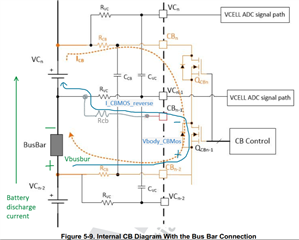
In other words we would to mount Rcb resistance, connecting the upper CB pin to the busbar, also in the channel used on busbar measurement (in gray).

Consider the situation in which the battery module is in discharging: the green current "Battery discharge current" flows from negative to positive battery terminal thus a voltage drop shown as "Vbusbar" is present across the busbar. This voltage drop makes that a current (in blue, named I_CBMOS_REVERSE) will flow across the internal CB mosfet. In particular through its body diode.

  1. Is this the "the forward biasing of the internal CBfet" that you are referring for in the SLVAE87 document and that must be avoided?
  2. This I_CBMOS_REVERSE is limited by the Rcb resistances (2 x 100ohm in our case). Based on oure estimation of the voltage drop on the busbar (Vbusbar), just a little current (< 50mA) will flow on the body diode.
    1. What is the maximum current that the body diode of the CB mosfet can support?
    2. There will be some issue if some limited current flows on it?
  3. It seems the same situation occurs also when using the external balancing mosfet, on the external mosfet's body diode. As there is only the balancing resistor that limits the current, this current will be higher. Howerer, from our simulation, it seems that this will be not destroy the ext. mosfet. If we can keep safe the ext CB mosfet, are there any counterindication in leaving the upper CB pin connected to the busbar?

Thank you,

Best regards

  • Hi Luca,

    I will try to answer your questions:

    1. Yes this refers to the forward biasing of the back-body diode. Our design does not recommend any current to flow through the back-body diode. As the conduction threshold for the back-body diode is 0.3V that means that the voltage developed across your BusBar has to be lower, which will determine the max current flow (For Example a 100uOhm shunt, max 3000A), or you can implement an external schottky diode with Vf_max < 0.3V in parallel to the back-body diode of the BQ device so that the external diode conducts all of the current.

    2. Similar answer to Question 1. We don't recommend any current flow through the back-body diode due to long term reliability.

    3. I am not really sure what this circuit looks like, maybe you can submit a drawing here, however the key point is that there is no current flowing through the internal back-body diode of the CB-FET in the BQ device.

    Regards,

    Viktor.

  • Hi Viktor,

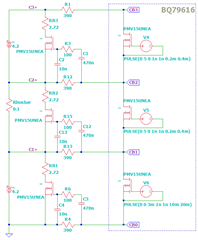
    This is the circuit I've in mind:

    I can use 390ohm CB resistors (R1, R12, R13, R4) so the CB body-diode current max. could be [Vcell-Vf(body_diode)]/2*Rcb=[4.2-0.3]/2*390=5 mA. I hoped this little current could be supported by the CB mosfets body diode but I undestand that TI probably has not tested this feature thus it cannot guarantee the long term reliability.

    Thanks for your precious reply.

    Regards,

    Luca

  • Hi Luca,

    I think you might have a mistake in the calculation i.e. the current through the body diode is [Vbus_bar - Vf(body_diode)] / 2 * Rcb

    I am also trying to make sense from your simulation:

     - Why is there an external Balancing FET on the Bus-Bar Channel ? This is probably not needed.

     - I am noticing that you are enabling V4 and V5 at the same time. This is not needed. In order to enable U5 you will only need V4/U2 to be enabled.

    Back to your original question, again we don't recommend any current flow through the back-body diodes of the integrated balancing FETs, no matter how small the current is. You can try this but at your own risk.

    Regards,

    Viktor.

  • Another thing I noticed on your simulation circuit... What are C1, C3 and C12 for? In our circuit we don't have these.

  • Hi Viktor,

    you're absolutely right, I've done some mistake. I'll try to clarify:

    I think you might have a mistake in the calculation i.e. the current through the body diode is [Vbus_bar - Vf(body_diode)] / 2 * Rcb

    Body diode current: It's correct your formula, [Vbus_bar - Vf(body_diode)] / 2 * Rcb but the key point now (for us) it's the estimation of the Vbus_bar max. This will be Rbus_bar*Ibatt_max but the Rbus_bar could be very high if the busbar is not connected in a strong way to the bus (i.e. one ore more busbar screws that are not tightened). But estimation is up to us. Thanks for your correction.

     - Why is there an external Balancing FET on the Bus-Bar Channel ? This is probably not needed.

    EXT Balalncing FET o Bus-Bar channels: Our idea is to design a unique BMS slave board (only one P/N) that is able to handle all types of battery module (e.g. 16 cells connected in series wit a unique busbar, 15 cells with 2 busbar, 14 cells with 3 busbar, etc.). So the ext.balancing FET are there but in certain cases we will use some channels as busbar sensing channel. Remove the ext mosfet circuits for some channels imply to have different BMS slave board P/N. This is difficult to handle for our company.

     - I am noticing that you are enabling V4 and V5 at the same time. This is not needed. In order to enable U5 you will only need V4/U2 to be enabled.

    Cell balancing handling (with busbar): Yes, you're right. This is probably because I copied the circuit from the figure 5-9 of SLVAE87 – FEBRUARY 2019 document in which the CB channel were disconnected from the cell/busbar and the activation of 2 adjacent channels were necessary.

    What are C1, C3 and C12 for? In our circuit we don't have these.

    C1, C3, C12: Absolutely right. Another error during the copy of the circuit to post the figure here... I'm sorry for the confusion created.

  • Hi Viktor,

    Are there any information other than the Vf_max=0.3V of the back-body diode of the CB mosfets?

    E.g. would be useful the If(Vf) at different temperature.

  • Hi Luca,

    No we don't have these as we do not recommend any current flow through the back-body diodes.

    Regards,

    Viktor.