This thread has been locked.

If you have a related question, please click the "Ask a related question" button in the top right corner. The newly created question will be automatically linked to this question.

TPS22901: Vout<<Vin in ON state and Vout>0 in OFF state

Part Number: TPS22901
Other Parts Discussed in Thread: TPS22902, TPS7A02

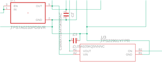
1) What issues would we face if Cout/CL (capacitance at output side/load side) is more than Cin in TPS22901 resulting in a condition of Vout>0 when the power source is removed. Would it damage the device or reduce its life?

2) I have the above condition and I am seeing that when Vin = 3.24V, my Vout=2.16V in ON state and when the switch is in OFF state I am seeing Vout=0.4V. Is this normal?

  • Hi Mayank,

    We recommend at least a 1:1 ratio between Cin and Cout to stabilize the input rail during high current draw events such as turn on. 

    With Cout > Cin, you are susceptible to to the condition of Vout > Vin. If you are intending for your Vout to be greater than zero when the power source is removed, I would recommend a load switch with a quick output discharge (QOD) feature such as the TPS22902 or to connect an external resistor to the load to discharge the output. However, consider that adding an external resistor will affect your rise and fall times. 

    If Vout > Vin, there is a possibility for reverse current to flow that could damage the device. However, the output has to be held high for long enough to turn on the reverse diode and consistently pump current back. If the load is resistive in nature, the voltage on the output can be discharged to GND naturally through QOD or an external resistor. 

    Best Regards, 

    Elizabeth 

  • Hi thanks for your detailed response, gives a lot of clarity. 

    1) Also I would want to clarify that once the power is on the Vin is held constant at 3.24V using a power converter/stabilizer so unless the power is switched off there isn't a case where Vout>Vin, its just when power is switched off that Vin becomes 0 while Vout was measured as ~0.4V and keeps dropping till it reaches 0. Is this normal behavior or is the hardware faulty?

    2) I am also seeing that in the same circuit, even when Vin is 3.24V I am getting a Vout of 2.16V, any idea on what could be the possible cause for this?

    Thanks,

    Mayank

  • Hi Mayank, 

    Could you share your schematic? That will help me understand what could be happening in the circuit.

    Best Regards, 

    Elizabeth 

  • TPS7A02 gives a clean output of 3.24V to VIN, C2 acts as output capacitor for TPS7A02 and also acts as input capacitor for TPS22901. C3 is the output capacitor for TPS22901

    For TPS22901:

    VIN = 3.24V (from TPS7A02)
    ON = 3.24V (gpio pin from a microcontroller)
    C3  = Cout = 1uF
    C2 = Cin = 4.7uF

    Vout is going out to supply a RF chip, this chip might have a capacitor inside it which may be greater than Cin, hence my original question of what happens when Cout > Cin. 

    Please note that the Load consumes an average current of 0.6mA with peak current consumption being 200mA for small burst of 10us which take place every 1 sec.

  • Hi Mayank, 

    Unfortunately, I cannot make any comment on the schematic you've shared as it does not illustrate the connections on ON and Vin and Vout. 

    A voltage drop such as the one you are seeing is not an expected behavior and could be due to several things. Is this error condition occurring across multiple devices and multiple boards? 

    Could you send me waveforms illustrating the error condition? 

    If output is held high for too long, the diode could be biased and reverse current could occur. This can occur if ON is left floating, as the device could be in an on, off, or partially on operation. 

    Best Regards, 

    Elizabeth

  • Hi Mayank,

    Since this thread is going on two weeks without a reply, I am closing/locking it. If there is another update here please make a new thread. 

    Best Regards, 

    Elizabeth