This thread has been locked.

If you have a related question, please click the "Ask a related question" button in the top right corner. The newly created question will be automatically linked to this question.

[FAQ] TPS61032: Burning out right when connecting battery

Part Number: TPS61032

Hello,

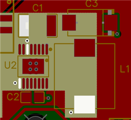
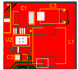
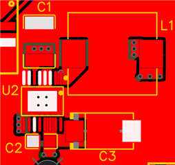
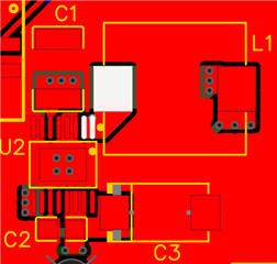
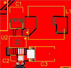
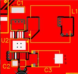
I am using boost converter TPS61032 in my circuit, but I find that after applying 3.7v from a lithium battery to its input, it immediately burns out and shorts the entire circuit. I am following the recommended design on its datasheet with the following values: L1= 6.8uH, C1=10uF, C2=2.2uF and C3=220uF (tantalum).

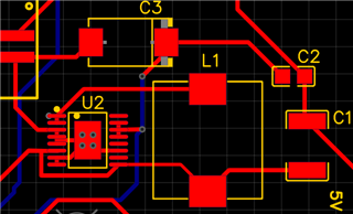
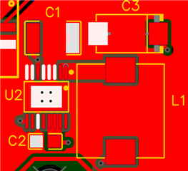
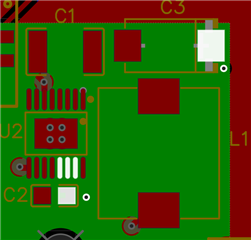
I read in other threads that the PCB layout its important when using this component, and I am wondering if it could be that some of them are too far from the IC. I don't understand how this could be causing a whole short circuit though. My tracks are 0.4mm wide.

This is the layout pertaining the TPS61032.

Thanks

  • Hi Manuel,

    You cannot just use single trace as power plane for any DCDC converter. This is a very undesirable layout. Please follow strictly per layout recommendation in EVM. Some notes below:

    1.The exposed pad under chip should be a solid ground and we strongly recommend 2nd layer to be ground layer;

    2.SW-VOUT-GND is a very important loop. If the loop is badly layout, both HSFET and LSFET of converter could be in danger of breaking down;

    3.All traces about SW, GND, VBAT, VOUT should use solid power plane/polygon; Trace is not allowed.

    -Wenhao

  • Thank you for your advise Wenhao. I'm going to try to improve the layout then. Why do you think this could be happening? Could there be some sort of spike induced by the layout?.

    On the other hand, I have also read in the tps61032 datasheet that the input capacitor (c1), inductor (l1) and output capacitor (c2) should placed as close as possible to the IC. Do you think there could be something about this in my current design as well?

  • Hi Manuel,

    The layout, especially the loop from VOUT pin->output capacitor->PGND pin is thin, long and contains vias. This would make excessive ESL, ESR into the loop and introduce large voltage stress to internal FETs. Also the VBAT, SW trace where could flow large current is very thin, this would make device operates abnormally and unpredictably by inducing noise inside the control circuitry.

    Please refer to EVM layout as the layout in datasheet uses QFN package. Yours is TSSOP.

    -Wenhao

  • Wenhao,

    Thanks a lot. Modifying the layout seems to have improved the circuit. TPS61032 is not breaking down now. The only issue I'm having now, is that it's output jumps from 4.6 to 4.9 volts. I'm using the fixed 5v output version. I suppose this has something to do with the output capacitor?

  • Hi Manuel,

    Please use tantalum capacitor with ESR higher than 30mOhm and effective capacitance larger than 22uF under 5V bias.

    -Wenhao

  • The output capacitor I am using has the following specs: 220uF (capacitance), 200mOhm 100KHz (ESR), +/-10% (tolerance), 10V (rated voltage) and it is a tantalum capacitor.

  • Hi Manuel,

    Thanks for clarify, could you please share me with your updated layout and waveform you took on VOUT? Thanks!

    -Wenhao

  • I am using 3 layers now:

    GND (see SW on this layer too: pins 1 and 2)

    VOUT

    VBAT

    I have not studied the output waveform as I do not have an oscilloscope. I noticed this fluctuation using a multimeter to measure the output voltage. The values I can see go from 4.6v to 4.9v. Once output gets to 4.9v it goes back to 4.6v and so on; this makes me think the issue has something to do with a capacitor, but I am not sure where the issue is.

  • Hi Manuel,

    One big problem i have seen now is why you just use a via for Vin of inductor? The input trace for inductor should be wide and solid. What is the output current when you have seen Vout fluctuation? Please share me with layout when you have updated Altium designer file before you shipped it out in factory.

    -Wenhao

  • Hi Manuel,

    For better boost layout understanding, you may need to go through below application note first. I see you may not have fundamental of how boost converter is operating. It is better you have some background knowledge for it before I go through the layout check

    Five Steps to a Good PCB Layout of the Boost Converter

    -Wenhao

  • Wenhao,

    Thank you for sharing that documentation. This is actually the first time I implement a boost converter and I didn't expect the layout to be so important, sorry for my limited knowledge about it. I have now modified the layout, following the tips in the document:

    GND

    SW

    VOUT

    VBAT

    C2 and C3 are the output capacitors. I placed them close to the IC, trying to use polygons; I believe they are wide now. Connections to the inductor are also wider now and have more vias. C1 is the input capacitor.

    Do you think this should improve the output?

  • Hi Manuel,

    Thank you for your effort modifying the layout. It always takes some time or even some pain to learn the experience. Please refer to below suggestions per your layout. This one is much more acceptable than previous one.

    Top:

    1.Please move L1 a little bit down so that SW trace becomes as short as possible. SW net is very noisy so we always want to make it small to mitigate EMI-related issues;

    2.Please add some GND vias near C1, C2&C3 gnd lead, to make it connect internal ground layers.

    3.What is capacitance of C2? 2.2uF is good;

    -Wenhao

  • Thank you for these suggestions Wenhao. I have moved L1 to shorten SW connection. I am a little confused about the GND vias you mention for C1 C2 and C3, given that there are no internal ground layers. All my GND layer is on top, so these vias would not connect to anything?. Yes, C2 is 2.2uF

  • Hi Manuel,

    I would recommend you put at least 1 or 2 intact internal GND layers, in order to mitigate EMI and provide better conduction of switching current. This is a best practical approach we usually do for DCDC power supply. If you have more questions, I would appreciate your initiate another thread in E2E. Thanks!

    -Wenhao