This thread has been locked.

If you have a related question, please click the "Ask a related question" button in the top right corner. The newly created question will be automatically linked to this question.

BQ25606: timing

Part Number: BQ25606

Dear team

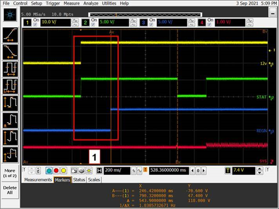
There are a few problems with the timing of BQ25606 during startup. The customer measured several points, IC input (12v), STAT, REGN, SYS.

Before the power enters the IC, /CE is already low. At this time, plug in the power again, STAT will have a high level delay of 800ms, and then STAT will turn to low.

1. In the first block, the difference between STAT and REGN is about 220ms. Is this time the REGN delay 220ms mentioned in the following spec(8.3.2.1)?

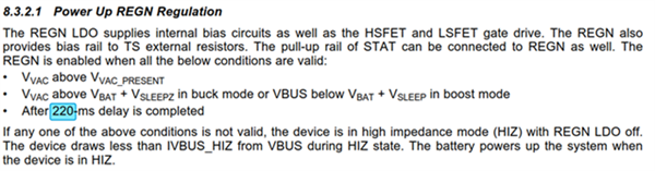
2. After the second block REGN turns to high, STAT remains high as well. This period of about 600ms, is there any mention in the spec?

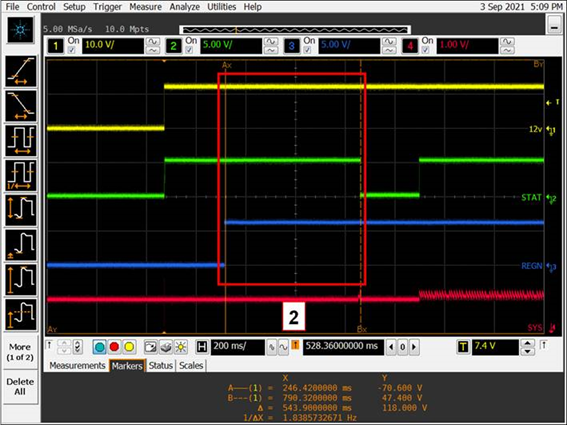
3. In the third block, you can see that STAT turns to low. Will the BQ25606 preset STAT turn to low, regardless of whether the battery voltage is fully charged or not Does BQ25606 use this low pulse to determine the subsequent output status of STAT? Is there a document description during this period?

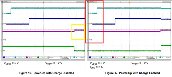
4. Is the Charge Disable in the left picture/CE pin high at the beginning? Why is SYS being elevated in charge disable in the yellow box? The SYS in the red box was already high before VBUS came in. Is the battery connected, so the SYS voltage is the battery voltage at this time?

Many thanks

Denny

  • Hi Denny,

    1. Yes, as you mentioned there is a 220 ms delay between VAC fulfilling the REGN power-up conditions and the REGN LDO being enabled. That is the expected timing according to the datasheet.

    2. This 600 ms delay is likely due to source qualification and Input Source Type Detection. What type of input source is the customer using for this charger, if USB what kind? This type source detection is better described by this video on USB BC 1.2

    training.ti.com/what-is-usb-bc-12

    3. STAT dropping indicates that charging has commenced, it is subsequently disabled indicating that charge current is below charge termination and battery voltage is above recharge threshold. This will occur if VBAT is close to battery regulation voltage. This period is necessary to sense that ICHG is below charge termination, since this part does not have an ADC to sense VBAT. This is a part of the autonomous charging cycle (8.3.6.1) .

    4. As you described, VSYS will be high as it is powered from VBAT regardless of whether CE is high or low, so long as VBAT is above VSYS min. In this case VSYS is approximately equal to VBAT minus the voltage drop across BATFET. Once VBUS goes high, the VSYS will be powered from VBUS causing the rise in VSYS. This is the case for both waveforms.

    Please let me know if there is anything I can clarify.

    Thank you,

    Juan

  • Hi Juan

    2. This 600 ms delay is likely due to source qualification and Input Source Type Detection. What type of input source is the customer using for this charger, if USB what kind? This type source detection is better described by this video on USB BC 1.2

    =>The input source of customer is 12V adapter, not USB.

    The customer would like to know. whether the The 600 ms delay is described on datasheet?

    Many thanks

    Denny

  • Hi Denny,

    The datasheet describes that following REGN LDO power up, the device will determine input current limit by undergoing input type detection (8.3.2.3) which includes USB data line detection (8.3.2.3.1). This process is described by USB BC 1.2, the specifications of which can be found here:

    https://usb.org/sites/default/files/USB_Battery_Charging_1.2.pdf

    As described in (8.3.2.3.1) non-standard adaptor detection is applied only after the Data Contact Detection timer expires, which as per USB BC 1.2 should be between 0.3 to 0.9 seconds. In this device, like some of our other devices, the timer has a duration of 600ms. Non-standard adaptor detection will likely return indicate that the adaptor is unknown in this case and input current will be determined by the ILIM pin.

    Please let me know if there is anything I can clarify.

    Best,

    Juan

  • Hi Juan

    According your reply:

    As described in (8.3.2.3.1) non-standard adaptor detection is applied only after the Data Contact Detection timer expires, which as per USB BC 1.2 should be between 0.3 to 0.9 seconds.

    In this device, like some of our other devices, the timer has a duration of 600ms. Non-standard adaptor detection will likely return indicate that the adaptor is unknown in this case and input current will be determined by the ILIM pin.

    The customer downloaded the file provided before, but they did not find the text in the second paragraph below. Could you help to mention the source?

    Many thanks

    Denny

  • Hi Denny,

    DCD Test specifications (with and without current source) are found in sections 7.3 and 7.4, (Pages 31 and 34 respectively) for the document provided.

    Please keep in mind that the test specifications are descriptive of the USB BC 1.2 are written by the USB Implementor's Forum, not by Texas Instruments. My notes on the TI devices are just a clarification on how TI implements that standard in their devices.

    Thank you,

    Juan