Hello Ti,
I have a few questions regarding the PMIC – P/N:TPS650861
- The PVIN3,4,5 input pins (Converters) can be 3.3V – 5.0V.I want to use 3.3V to PVIN3,4,5 input pins. The data sheet not support the efficiency in case of PVIN3,4,5 connected to 3.3V only 5.0V.
Could you send me this information? Is their any advantage to connect to these pins 5.0V and not 3.3V? If I will connect PVIN3,4,5 to 3.3V – I will connect LDO5V output to the DRV5V_x_x inputs.
- For programming OTP memory, IRQB and CTL4 pins should be connected to 7.0V.I need to use 7.0V power supply. What is the maximum current from this 7.0V power supply when programing the OTP memory?
- Is their any option not to use any of CTL1-CTL6 and the PMIC will start enable the power supply immediately? I don’t want to use another/external power supply to enable CTL1-CTL6.
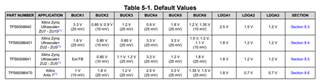
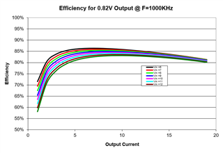
- BUCK1,2,6 – DC output voltage accuracy. According to the data sheet the accuracy I +/- 2% for Vout=1.0-3.3V @ 100mA to 7A. In case I want to use Vout=0.82A @ 10A.What is the DC output voltage accuracy in my case?
- The TPS65086x Evaluation Module board includes diode (D7 refence designator) to CTL4 pin. Could you explain why do we need this diode?
- Only Buck 2 and not Buck1,6 includes FBGND2 (negative feedback) pin. So I guess that Buck2 should be the strong buck in the PMIC. Right?
- The OTP memory is loaded into the corresponding volatile registers which are then used to control the PMIC. After that all the power supplies enable using the OTP, Can we use the I2C interface to fine tuning the output voltages of the PMIC by write to registers?
Thanks,
Moshe