This thread has been locked.

If you have a related question, please click the "Ask a related question" button in the top right corner. The newly created question will be automatically linked to this question.

LM63615-Q1: What is the cause of the failure?

Part Number: LM63615-Q1

Hi Team!

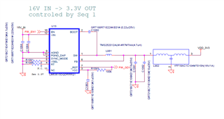
I designed the circuit as shown in the figure below, but IC destruction occurs frequently. 8pcs./20pcs.

There is no output from the SW and it is generating heat.

Maybe the output FET is broken in short mode.

What could be the cause?

postscript. The specification says that the VIN is 3.5V ~.
What happens to the VCC output at that time?
I don't think the LDO output 5V can be output.

  • HI

    do you know when the device be damaged? what is the C1058 and C1059 value? and can you share the layout?

    Tks

  • Hi

    C1058 -> 4.7uF  C1059 -> 220nF

    >do you know when the device be damaged?

    I don't know when it broke.
    It worked normally, at least immediately after the power was turned on.
    While I was doing the experiment, maybe  Energizing time is a few hours, The number of on / off is about 10 times

    it broke before I knew it.

    There are no errors such as shorting with a tester.

    Was there a timing when the input voltage became higher than the output voltage when the power was turned off?

    I suspect that,

    but I have stopped turning on the power because I'm afraid that it will break any more.
    In that case, the spec sheet says to insert a Schottky barrier diode.

    However, I am looking for a Schottky barrier diode with a VF of 0.3V or less.

    The foot print is below

  • HI

    do you only have C1058 and  C1059 at input side, is there no any other capacitor between input and input voltage. and if you power up the device, can you measure the input pin voltage and SW voltage ?

    Thanks