Other Parts Discussed in Thread: TPS561201
Hello,
So I needed to know if TPS561208 can be designed for supporting 15V Vin, as mentioned in the datasheet it can take upto 17V (recommended), 19V (Absolute Max), with the SW node supporting upto 19V and 21V of 10ns transient.
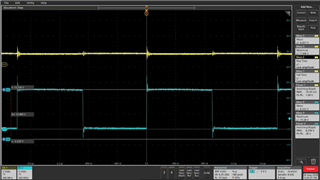
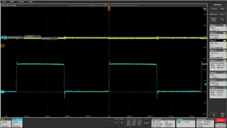
So in our design with the IC, at 15V Vin, the observed transient during switching is going upto about 19V for about 20ns at low loads and 16-17V at 0.5A load, it is also possible that the actual is lower given the probing error. Wanted to understand this behaviour better, why the switch node ringing reduces with load.
The typical load for our application would be less than 0.5A in which case the observed transient voltage at the SW node would be present, wherein there wouldn't be sufficient margin. Also in the datasheet some of the test conditions is mentioned to be at 15V Vin as well, wanted to know the reliability of the IC at this condition, possibility of failure especially when the Vin max is mentioned as 17V. From observing the SW node ringing at 15V Vin doubting whether it can be designed for the said 17V Vin.
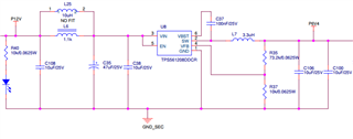
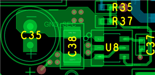
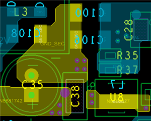
Just to add, the layout was designed very similar to the recommended layout in the datasheet.
From the Datasheet was comparing the TPS561208 and TPS561201, and in TPS561201 has the pulse skipping at low loads and the TPS561208 doesn't, so does this reduce the SW node ringing ?
Could you please clarify the above mentioned points, please ?
Thanks & Regards,
Rohit.