This thread has been locked.

If you have a related question, please click the "Ask a related question" button in the top right corner. The newly created question will be automatically linked to this question.

LM5046: LM5046 application design detail confirm

Part Number: LM5046

Dear  Expert ,

Good day!

Our customer using a LM5046 PSFB with these conditions : 

- Current mode control

- External SYNC

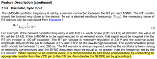
In this case, TI recommends to ground the SLOPE pin and to put a resistor for slope compensation between VCC pin and CS pin in the datasheet 7.3.5.  But it seems like  the CS pin is not supposed to bother about slope compensation whereas the RAMP pin should but nothing is said about RAMP pin.

On all application designs, the RAMP pin is linked to the CS pin with a resistor but never have I seen a resistor between VCC and CS !

My question is : in case of external sync in current mode control, if we ground SLOPE pin, how should I manage the RAMP pin and the CS pin ? 

BR,

Leon.liu

  • Hi,

    You use a current mode control which usually needs slope compensation, so SLOPE cannot be grounded in this case. You need to follow Fig 11 on page 16 to make your design. You may also refer to the LM5046 EVM on the below link of its schematics.

    www.ti.com/.../snva470

  • Thanks for answer,

    But then why does the datasheet states : "When the RT pin is synched to an external clock, it is recommended to disable the SLOPE pin and add slope compensation externally by connecting an appropriate resistor from the VCC pin to the CS pin."

    I do use the RT pin synched to an external clock so should I just ignore this ?

  • Hi,

    yes, ignore it and follow what I described to you based on the datasheet fig 11 and the EVM circuit.

  • M.Huang, 

    Thank you for the reply.

    I am little bit concerned though as in the company I work for, I have to thoroughly detail my designs in terms of hardware conception and going against the datasheet is strongly not recommended.

    Is there an issue in the LM5046 datasheet with that 7.3.5 section ? 

    If yes, is there any slight chance a revision of this datasheet can be issued, which would help me justify the use of the circuit you advised me to use ?

    Sincerely, 

    Grégoire OLIVES 

  • Hi,

    There is no issue on the datasheet. You can follow the datasheet by short SLOPE  to ground and using the recommended external approach. The way RAMP connection is still the same as shown in Fig 11 and in this case tie a resistor from VCC to CS pin and disconnect SLOPE pin from the current connection then ground it, as show in Fig 11 (b). 

    The recommendation is actually to help reduce possible noise from SLOPE back to CLK. The practice from EVM or the designs from customers shows ok to still use SLOPE on chip and no need to use the recommended external approach that is ok and without noise issue.

    So you can do either. But if your design has possible high noise then you can follow the recommended approach.

    In case you short SLOPE and use the recommended approach, you need to make sure VCC in good regulation so to maintain your external slope compensation current in good regulation.