This thread has been locked.

If you have a related question, please click the "Ask a related question" button in the top right corner. The newly created question will be automatically linked to this question.

[FAQ] UCC21520: The impact of changing FETs without modifying the gate drive circuit

Part Number: UCC21520

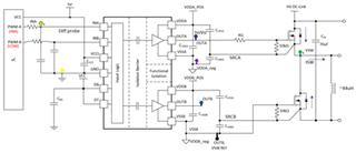
What should we take into account when changing a FET? What components should be modified and how could this affect our overall system performance?

  • Designers may want to change FETs for multiple reasons such as shortage in devices, change in the system specification, or trying to increase system performance by changing specifications such as switching frequency. However, when designers swap out FETs without modifying the gate drive circuit, they unknowingly can cause drastic changes in the application performance because the dynamic characteristics of their FETs (RDSON, CISS, COSS, internal RG) change between FET part numbers. It is well known that gate resistors are crucial for limiting noise and ringing in the gate drive path, but did you know that gate resistors affect more than just that? Changes in gate resistance affects the FET's gate charging current which directly affects the drain to source voltage slew rate and overshoot on the switch node. Faster dv/dt does help reduce switching losses, but designers must limit the peak switch node slew rate to within the max dv/dt specification of the gate driver's level shifter and limit switch node overshoot to within the breakdown voltage of the FET. Higher gate resistance comes with the unavoidable tradeoff of longer switching times and increased switching losses, but lower switch node overshoot. If the gate resistance is too small the gate driver is subject to large overshoot voltage at the switch node, but faster switch speeds. 

    Test Set-up:

    The data below was measured using high side double pulse testing, where INB is held low as INA is fed a PWM signal, switching the high side FET on/off. The load is an inductor tied from the switch node to PGND. The first pulse builds up current in the inductor up to a designated threshold and the second shorter pulse is only used to measure the turn on characteristics of the FET. 

    Double pulse test setup:

    Figure 1: Double Pulse Tests Schematics 


    Figure 2: Double Pulse Waveforms

    Measurement Data:

    The below data in Figure 3 was taken with the same gate driver with +4A/-8A typical gate drive strength, with 0 Ohms of external gate resistance, and at room temperature. Several different 1.2kV SiC FET samples in TO-247-4 packages were tested with recommended datasheet drive voltages under the same switching current across different bus voltages, and it can be observed that each has a unique peak slew rate curve across bus voltage. These curves reveal the drastic differences in dynamic performance between FETs, and highlight the need to treat all as unique. As previously stated, the circuit designer must limit the peak switch node dv/dt to within the specification of the gate driver level shifter circuit. 

    Figure 3: Max Turn ON and Turn OFF

    Common Mode Transient Immunity (CMTI) is a fundamental parameter to consider during the design of gate drivers that operate at high switching frequencies. When the switch node has a rate of change that is above the datasheet values, it is possible that the driver can experience logic errors, where the output can glitch high or low under high slew rates. In this case study, we will examine the gate resistance required to limit the switch node overshoot to <1100V, and the dv/dt to < 100V/ns (Figure 4). We can see that for bus voltages in the 500v-700v range, higher gate resistance (>10 Ohms) is extremely effective at keeping dV/dt near 100V/ns compared to smaller values (<5 ohms). Voltage overshoot is also heavily impacted by external gate resistance, in the 300-600V VBUS range, we can see an overshoot as high as 300-400V for low gate resistance (<5 Ohms).  It is important to remember that FETs will likely switch even faster at low temperatures and RG should be optimized across the required temperature range of the system.   


    Figure 4: Overshoot and Max Switch Node Turn ON dv/dt for Sample B

    Figure 5 below shows the various ranges of overshoot across several different SiC part numbers with no external gate resistance. Similarly, each manufacture's FET contributes varying degrees of switch node overshoot. The faster switching FETs tend to have larger overshoot, and at 600V, the largest overshoot measured was 600V. Without external gate resistance to reduce the overshoot, that additional 600V could cause breakdown of the SiC FET, which has a Vds breakdown of 1200V.  

    Figure 5: Switch Node Overshoot