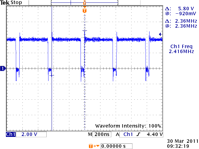
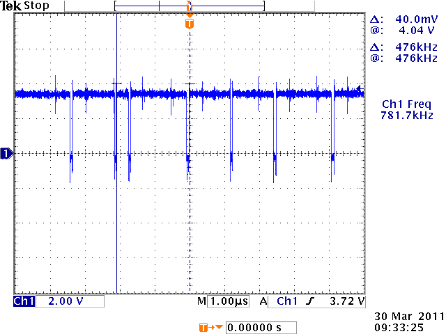
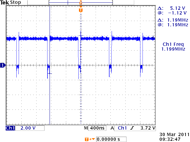
This thread has been locked.

If you have a related question, please click the "Ask a related question" button in the top right corner. The newly created question will be automatically linked to this question.

TPS63020 VIN=4.1v and VOUT=3.3v SW waveform

Dear team:

As you can see form below waveform, it is the switching waveform on our EVM board.

The test condition is VIN=4.1V and VOUT=3.3V.

The switching waveform seems like unstable when load condition over 1.5A, is it correct?

If the maximum load condition of my customer is 2A, any risk for this unstable switching waveform?

VIN=4.1V   VOUT=3.3V   IOUT=2A    on EVM board

VIN=4.1V   VOUT=3.3V   IOUT=1.5A    on EVM board

VIN=4.1V   VOUT=3.3V   IOUT=1A    on EVM board

  • Hi Redick, 

    Two things to note in looking at the waveforms above:

    1)       As the load increases, the high level switch node voltage decreases because of the voltage drop across the control fet increases.

    2)       Also, the frequency is decreasing because less buck pulses are needed to regulate the output voltage.

    If you were to measure L2 node as well, you will see that it should be switching too. This is evidence of the IC switching between buck and boost mode to regulate the voltage.  When Vin is close to Vout, the IC will automatically switch between buck and boost modes to keep Vout regulated.

    The switching waveform is not unstable, but behaving as expected from experiencing some losses across the board and in the ICs FETs. Also, remember to measure the input voltage at the J2 header on the EVM (across S+ and S-). The voltage drop from the input supply to the IC can be several hundred mV.

    Regards,

    Sheronda