This thread has been locked.

If you have a related question, please click the "Ask a related question" button in the top right corner. The newly created question will be automatically linked to this question.

LMR36015: Wont reliably start up in the inverting buck boost configuration

Part Number: LMR36015

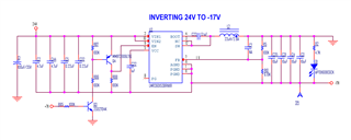
I built an inverting buck boost regulator using an LMR36015. It is converting +24V to -17V. It won't start from a fully-off state. When I turn off power there is a brief burst of operation. If I reapply power while it is generating -17V it will continue to run. Here is the schematic.  The design values were obtained from the TI web based power supply design tool.  I have tried adding a reverse clamp on the output using a Schottky diode. It did not change the behavior.

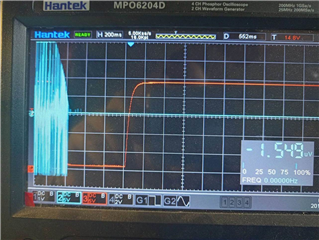
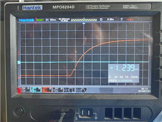
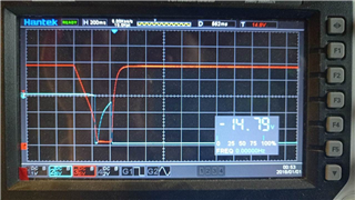
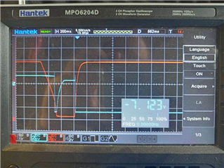
Condition: shown regular case, -17V doesn’t start.  RED: 24V input BLUE: -17V 

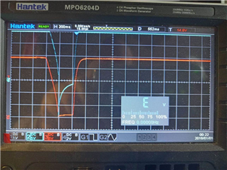
Condition shown: -17V works fine after power cycling,  RED: +24 input BLUE: FB pin 

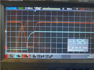
Condition shown: -17V was operating well, toggling input power quickly and it continues to run. RED: +24 input,  BLUE: -17V 

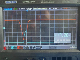
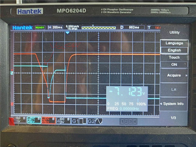
Condition shown: -17V was operating well, toggling input power with delay and it won't start,  RED: +24 input,  BLUE: -17V 

Condition: captured on power recycling, after this switch -17V starts operating -17V – BLUE,  24V input – RED

 VCC pin – BLUE,  24V input – RED

ENABLE: – BLUE,   24V input – RED

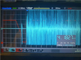
Condition shown: U3 starts working after power cycling,  RED: +24 input,  BLUE: SW pin

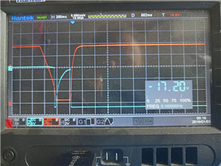
Condition shown: U3 doesn’t work after power cycling,  RED: +24 input, BLUE: SW pin 

  • HI

    there is certain possible issue caused Vo don't raise up

    1. what is EN PIN voltage in different scenario . Whether EN voltage make device can't power up?

    2. what is load condition, any chance to trig the OCP. As inverting buck boost topology, Lower Vin will have Lower output current limit. so if Vin start raise up from low voltage, and load is CC load, it is possible for converter to trig the OCP. but it will try to restart, so you will see SW keep switching after certain delay (150ms) when Vin raise up to 24V.

  • The circuit was unloaded.  Its normal load is on a different PCB.  I have also added a 1k Ohm load resistor at the output.  The behavior is unchanged.

    The EN pin is near 24V even when the part won't start.

    I don't actually have a board yet.  The above measurements were made by someone in a different one of our offices where the board was assembled.  They will be sending me a board early next week so I can work on this problem directly.  In the mean time I can request that he make whatever measurements you need.

  • When it is not running it does not attempt to start.  It only begins to run when power is turned off and the input slowly decays.  Look at the second photograph.

  • HI Cabot:

    Yes, I think it may related to the EN or other latch up function. cause OCP will make the device try to start up again, so that you can see the SW at least. but from your waveform, it looks the no SW, so I think it maybe caused by EN or VCC UVLO.

    Thanks

  • The problem does not appear to be the EN pin.  At my request the person testing the board connected the EN pin to a physical switch.  The behavior is unchanged.  He also tried running the unit from 7.9 to 25V and saw no change.  The only way it will start is by reapplying power as the unit goes through its burst of operating as it shuts down. 

  • Hi Cabot:

    is below the VCC voltage waveform ? it looks VCC is lower than 4V when the Vo is abnormal. Do you place VCC cap close to VCC pin and AGND pin.

  • The green trace is the output voltage which is supposed to be -17V. The red trace is the input voltage.

    The green trace was measured before adding the reverse Schottky diode so it was able to go positive when the regulator was not working.  Adding the diode did not make the switcher start.

    They have powered up more boards.  Some work correctly every time power is applied.

    They are sending me one board that reliably works and one board that exhibits the misbehavior shown in the post.  I expect to have them by the end of the week.

  • HI Cabot:

    The picture I attached the green one I think is VCC as you mentioned above. when Vo=0V, VCC=4V. After Vin(red trace) power up again. the Vo should build up to -17V, and Vcc=5V, so that we can see the green one is -17V+5V=-12V. 

    so when VCC turn below than 4V should be the key that Vo can't be powered up.

    If you have board, pls help monitor the vcc when it can't build up to 5V

    Thanks

  • I understand that it won't power up when Vcc is too low.  However Vcc is created on the chip so why isn't it high enough?  The chip has 24V applied to it.

  • Hi Richard, 

    Can you please try connecting EN directly to VIN and see how the part works on power-up?

    Also, can you please share your board layout?

    Thanks!

    Denislav

  • The person who has been powering up the boards told me he tried that and it didn't help.  UPS is supposed to deliver a pair of boards to me on Monday.  I will be able to make measurements myself then.

    I've attached images I captured from the Cadence viewer.  It is a 10 layer board.  The images are in layer order.  The silk screens are at the end, bottom first.


  • OK, thank you. We will review the layout and provide some comments by then. 

    Cheers, 
    Denislav

  • Once I received a board I could evaluate myself I discovered that the problem is due to a excessive solder paste during assembly.    The board I received exhibited the same symptoms as the one examined by the other engineer.  

    The regulator would start briefly when the +24 was switched off.  If I reapplied power while the -17V led was lit the supply would stay running.  If I tried to start it normally it would not start.  Tying the EN pin made no difference.  I noticed that the Vcc voltage never got above 2.5V which is less than the regulator needs to function.  When I measured the resistance from the Vcc pin 5 to ground I found it measured 70k Ohms.  The boot pin 4 measures 50k to ground so it’s possible the short was to that pin instead of ground since there is no ground near pin 5.  It’s also possible the problem was a bad chip but since it occurred on several boards I don't think it's likely to be bad chips. Solder issues are more likely.

    I think what was happening is that the resistance to ground was low enough to drain the current that normally went from the +24V input into the internal LDO.  That kept the LDO from getting to the +4V required for the regulator to start.  When the +24V was turned off the Vin voltage dropped quickly but since the input capacitors (C2 and C44) were charged to 24V they pulled the regulator output negative until they had time to discharge.  With the output negative the resistance from the Vcc pin to ground provided a current into the Vcc terminal that powered the LDO and allowed the chip to start. 

  • Thank you for this update Richard. 

    Have you tried reflowing the part to confirm it is a soldering issue?

  • I replaced the part.  It's too difficult to solder for me to risk just reinstalling the one that was there.

  • Understood. Thank you Richard. I will close this thread for now. If there is another issue on this topic, please respond here and we can re-visit. 

    Regards, 

    Denislav