This thread has been locked.

If you have a related question, please click the "Ask a related question" button in the top right corner. The newly created question will be automatically linked to this question.

UCC27282: Lo Side Driver Failures - Update 2

Part Number: UCC27282

Hi,

This is a follow on from my last two posts.

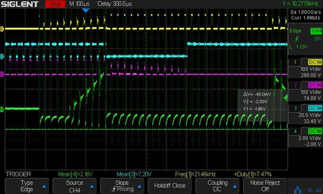
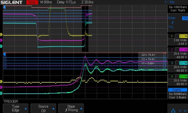
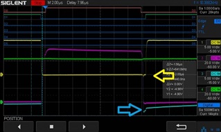
We have been testing our inverters various power levels and achieved another failure, even with, what we consider a reasonable layout, and including protections such as the additional Schottky diodes.

In our weeks worth of testing, we have had many high power runs with the inverters powered from 60 VDC, there have been no issues.

Today we increased the voltage to 72 VDC, and before our motor had even completed a single revolution, we had a damaged UCC27282 device.

The device exhibits the following:

1. High Current Draw

2. LO output stuck high (at VCC)

3. HI output inop.

4. No charge pump capacitor voltage.

Is there anything additional TI can add as to why these drivers are so sensitive to failures when used in a motor drive application?

We will try next to remove the current sense resistor system, as this could be causing issues.

Thanks.

  • Hello Stomp,

    By the description of the failed device behavior, is sounds like there were failures on the low side driver, specifically the pull up internal device on the driver output. I looked back at previous threads and I see we recommended trying addition of clamp schottky diodes from the driver output to VSS, since in many cases there is driver output voltage undershoot which may cause issues.

    By the description of this failure, it sounds like there could be excessive driver output overshoot, to improve the robustness of the driver we recommend adding schottky diodes also but from LO to the VDD pin to limit the overshoot on the LO output. Let us know if you see any change with the removal of the current sense resistor experiment you mentioned.

    Regards,

  • Thanks again for your support on our project Richard,

    We've removed the shunt current sense resistor from our design.

    In a previous post, we had a discussion about the observed negative value on the HS pin, and at the time I considered it only a function of our power supply setup.

    Since that post we are have moved to a fully isolated and floating power supply setup for the inverter, powered from a large battery bank.

    I've just captured a scope trace showing the voltage at the VS pin, as measured directly at the pin using a RF SMA connector. It looks like we have large negative voltages on the VS pin. I would expect to see some negative spikes here for a very small duration as the freewheeling current is absorbed by the diode in the lower FET. However as can bee seen below, a large portion of the phase is below zero.

    Below: Green - VS Pin measured at device, other colors are gate signals.

    As the DC link voltage and motor RPM increase, these values get quite large, and I could easily see the -HS transient value being exceeded, as well as the HS-HB voltage maximum of 20V if the negative spikes integrate across the capacitor.

    There is mention in the datasheet (8.2.2.7) about extra transient protection. I think our next point of call will be to add a 2R resistor in series with the HS pin, and maybe an additional schottky diode between GND and HS, but I'd have to find one with a large enough voltage rating.

    I'll post back when the boards are patched.

    Thanks.


  • Update from todays testing.

    1. Added 2.2R in series with VS.

    2. Removed current shunt sensors

    3. Diodes from GND to LO and HS to HO Still in place.

    At 60 VDC, motor starts and runs well up to our design target of 15K RPM / 20A

    At 72 VDC, instant gate driver failure as soon as the PWM is enabled.

    I will repair hardware and try for another diode from LO to VDD.

    Thanks.

  • Hi,

    This is the third update from testing.

    All of our attempts to date have resulted in destruction of the gate driver at 72 VDC, whereas they survive fine at 60 VDC.

    Our attempt last night focused on fitting a diode between LO and VCC. Again the design runs perfectly at 60 V, and we achieved a full duration motor run.

    We have a 2R resistor in series with HS, we have a diode between GND and LO, and another between HS and HO. We have a third diode between LO and VDD also.

    When we apply 72 VDC to the inverter, at or about the first few PWM pulses, the gate driver failed. Because we had fitted a diode between LO and VDD, the bypass capacitors to he gate driver smoked, and our floating power supply was instantly destroyed.

    Somehow, the LO pin fails in such a way it goes way above VDD, and I would suggest it goes as high as our 72V VDC supply for the inverter and hence the instant destruction. There are series resistors, currently 10R between the low side FET gates and the LO pin, so even if somehow the low side FET's failed, I would expect the gate resistors to open circuit first. From the failure condition that we have constantly been seeing, I can only draw the condition that the LO pin fails within the device, and there is not an external influence specifically causing destruction of the LO.

    This is probably our tenth inverter design our company has attempted over the years, we are just totally lost as to why the gate drivers keep failing at high voltage.

    TI: Is there anything else we can try at this point? We are really stuck here.

    Thanks.

  • Hi,

    4th update for today.

    So we setup an experiment, diving only a single pair of FETs with HS connected to one motor terminal, and the other grounded.

    We start off with a small amount of PWM, and increase it somewhat. At 60V we have nice clean waveforms, everything is good.

    At 75 VDC, at the very first PWM pulse we get an explosion, with the lower FET cracked, and the gate driver failed.

    The moment of destruction is shown below:

    1. Yellow - LO

    2. Pink - HI

    3. Blue - HS, Green = Motor Terminal

    I think its probable that the lower FET has switched on. I did not have the scope down low enough, but the upper FET was absolutely on at this point.

    So things brings to the question, is the failures we have been seeing the gate driver not holding the LO pin low enough for our VGS_thresh of min 2.0V.?

    Thanks

  • Hi Stomp,

    Thanks for all the information provided, I'm reviewing this and will get back to you. On the last plot you provided, is the pink signal really HI pin (high driver input), or did you mean HO pin (high driver output)?

    Best regards,

    Leslie

  • Hi Leslie,

    Thanks again to you and Richard for your continued support.

    I think we are getting much closer to narrowing down the cause of the problems we've been seeing.

    To answer your above question, yes the pink is the HO output. Sorry for the terminology issues.

    Last night we built a new batch of inverters and fitted 1.5K pulldown resistors between gate and source of all our FETs. Magically our LO side gate waveforms now stay below the Vg_th value of our FETS and the gate ringing, which we are pretty sure was caused by the LO FET's switching on for an instant is also gone.  So I think this is one issue fixed.

    Today we did a moderate power run, 60 VDC bus voltage. I've attached a screenshot below showing the performance with Gate-Source resistors fitted, along with the two Schottky diodes, and no current sense shunt as per previous posts.

    Again, these waveforms are taken as close as possible to the devices, using RF-SMA connectors.

    D0, D1 = PWM H and L

    Yellow = LO (at FET Gate)

    Green = VDC Bus (At Battery),

    Pink = HO (at FET Gate)

    Blue = HS (directly at the gate driver / top of the Cboot cap).

    I note that we have a small negative pulse on the LO side (yellow) with the pull down gate-source resistors fitted. This could be of no issue as we are switching quite a bit of current at this point. And we have a small blip in the VDC Bus (Green) trace which could just result from the change in voltage due to the power supply inductance during the dead-band period. We will have to do a detailed study of this pulse later on.

    However the HS (Blue) is our major concern here. What is shown in the above plot is one third of a 3 phase inverter with the high side FETs activated.

    At the point on the scope capture at the blue arrow we see:

    1. The HS pin go to about -4.0V. And we note that this pin goes more negative with additional current consumption and a higher VDC bus voltage.

    2. The pulse width of the lowest voltage 'blip' on the HS pin is greater than the 100ns value in the datasheet for -14V.

    3. It would be likely to violate the -10V Vhs limit when we apply a much higher Bus Voltage / phase current.

    4. The HS pin is absolutely negative at this point, and the LO gate driver is on, hence the HS should be at VSS as you can see HO is at VSS at the point of the yellow arrow.

    I'm wondering if you could shed some light as to what I am seeing in the blue trace at the arrow on the screen capture.? I get the feeling that the "blip" at the blue arrow, could either be the natural FET switching cross-over, or Cboot recharging?

    I am also wondering what structures are inside the driver that I could further protect externally?

    For example if I (re)placed a small 2.2R resistor in series between the driver's HS pin and the FET's would this resistor limit enough current flow into the gate driver to prevent damage, or would I need to add, for example, and external diode between VSS and HS with the 2.2R resistor in place to absolutely protect the driver?

    Thanks again for your time!

  • Hi Stomp,

    Thank you for sharing your latest findings. I'm glad you were able to solve the ringing issue at the low side gate. 

    Regarding the negative transient on HS pin, switch node undershoot can occur when the load continues to draw current as the high-side FET turns off, forcing current through the freewheeling diode of the low-side FET, which induces a negative voltage. This can be caused by parasitics inductances on the traces and can potentially cause the bootstrap cap to be overcharged. 

    Slides 7 to 9 in this technical document talk in detail about switch node negative spike and recommendations to reduce it: https://www.ti.com/lit/pdf/slyp766?keyMatch=JACKIE%20HUI

    This FAQ explains this in details and has recommendations to avoid bootstrap overcharge: https://e2e.ti.com/support/power-management-group/power-management/f/power-management-forum/931493/faq-ucc21520-what-do-i-need-to-know-about-bootstrap-overcharge-when-designing-a-driver-bootstrap-supply?tisearch=e2e-sitesearch&keymatch=overcharged%20bootstrap#

    Other than the transient, the duration of the negative voltage on HS is a concern. Could you explain what is going on on the converter during this time?

    Please make sure that when HS pin is negative, the conditions mentioned in datasheet section 7.3.6 "Negative Voltage Transients" are followed. It would be good if you monitor HB voltage as well to check these conditions. 

    Best regards,

    Leslie

  • Thanks Leslie,

    Thanks document slyp766.pdf was very informative.

    The blue arrow on our previous scope capture is the reverse recovery charge from our FET's, as described in a few papers we have found. There is nothing we can do about this, other than to say our PWM method for commutation is to switch on the low side FET inverse to the high side FET in a "balanced mode", such that we use the Rds_on of the FET, rather than rely on the body diode (which dissipates more heat). This is opposed to using only "upper modulation" as seen in several BLDC trapezoidal motor drive control papers.

    I conducted another test last night, and achieved a full power / full duration run on our motor dive.  I monitored HS very closely, and at full power I only got to -6V, which is still within the limit.

    So I'll mark this as solved, thanks again for your help.

    To anyone else that has similar issues here is what I'd suggest based on my experience with this gate driver:

    1. Make provision for Schottky diodes between VSS and LO as well as HS and HO.

    2. Make sure you have gate-source resistors fitted.

    3. Tune your gate control resistors while monitoring HS, LO and HO to ensure they stay within parameters. You can only do this successfully with decent measurement techniques, so build these measurement systems (i.e. U.FL RF connectors) into the first design.

    Cheers

    Stomp!