This thread has been locked.

If you have a related question, please click the "Ask a related question" button in the top right corner. The newly created question will be automatically linked to this question.

UCC27714: Two-Switch Forward Converter design is a toaster.

Part Number: UCC27714
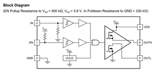
Other Parts Discussed in Thread: LM5112, UCC27322, UCC27532

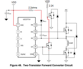
In Figure 49 of the data sheet for the UCC27714, an application for the device in a two-switch forward converter is shown. Whereas I agree with the general concept the author was trying to convey, the implementation of the concept per the figure is poor.

In Figure 49 of this application note, the Rboot resistor is in the drain lead of the signal switching MOSFET on the bottom -

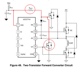
Typically, the Rboot resistor (if used) is 2.2 to 10 ohms or so. When the lower signal MOSFET turns on when the LO output from the UCC27714 goes active, to cut off the second MOSFET which is providing the ground path for Cboot, the lower MOSFET promptly blow up with a dissipation in excess of 12W and Rboot, with catching fire. Good times!

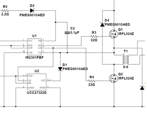
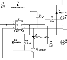
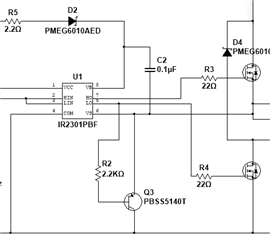
I have redesigned the circuit, and used an alternate controller IC (which is available from stock) and it works fine but I would not build it as it was described in the application note.

  • Hello Lauren,

    thanks for the input. I was concerned about this and ran a simulation. It is true that using a small boot resistor here of 2.2 to 10 ohms is likely too small. However, I was able to use a bootstrap of 20 ohms with no problem at 1MHz Fsw. With the higher value of a bootstrap resistor, the power dissipated became much more reasonable. Would you mind sharing how you redesigned the circuit? Also, do you have a question about this or do you just want to let us know you see a problem? 

    thanks,

    Alex Mazany

  • If a 20ohm resistor is used with a VDD of 15V, the current in Rboot is 750mA at 100% duty cycle, with a power dissipation of 11.25W, so with operation up to 50% duty cycle (as in a flyback application) a 10W resistor would be required, dissipating 6W -- and it would still be a 125°C toaster. I do not agree with your simulation analysis, unless you like toast. There is no reason to dissipate 6W in the design.

    This would be one possible revision with much lower dissipation -


    I primarily wanted you to know that I 'see a problem' with it. Several people on the Web have referenced this design for two-switch forward applications and may be using it for the basis of the work. I also initially reviewed it for the basis of a two-switch flyback design that I am working on, when I noted the design issues with it.

    In my current design, I used a fast, integrated dual MOSFET (BUK9K52 series) with low-Rdson as the logic inverter MOSFET and the bootstrap capacitor sink MOSFET to reduce the parts count and the size.

    If the transition speed is an issue at high frequencies, a single channel non-inverting MOSFET gate driver (MIC4452) can be used in place of the LO signal logic inverter MOSFET, thus sourcing and sinking the gate of the bootstrap low-side MOSFET, resulting in snappier transitions.

    Alternatively, the entire phantom half-bridge logic chain could be replaced with an inverting MOSFET gate driver with a high current output (IR4426, TC4426 or MIC4451) and high voltage switching capability. However, this option limits the final MOSFET rail to the maximum VDD of the gate driver (usually 12-18V). A small selection of alternative gate drivers could enable operation at slightly higher rail voltages (up to 35V) with this approach.

  • Thank you for your input. I agree, the revision you showed massively reduces the amount of power wasted in the bootstrap resistor. It works great in my simulations also. I'll be sure to inform the technical documentation team of this issue with the example design.

    thanks again,

    Alex M

  • I wanted to correct my comment -

    If the transition speed is an issue at high frequencies, a single channel INVERTING gate driver (IR4426, TC4426, MIC4451, etc.) could be used in place of the LO signal logic inverter (first stage) MOSFET, thus sourcing and sinking the gate drive of the bootstrap low-side (second stage) MOSFET, resulting in snappier transitions.

    Alternatively, the entire phantom half-bridge logic chain could be replaced with an NON-INVERTING gate driver (UCC27322, LM5112, MIC4452, etc.) with a high current output and high voltage switching capability. However, this option limits the final MOSFET rail to the maximum VDD of the gate driver (usually 12-18V). The extra diode (D1 below) is still required to prevent the gate driver from sourcing into the output section.

    A small selection of alternative gate drivers could enable operation at slightly higher rail voltages (up to 35V) with this approach. The IX4427, for example,  would allow sinking of the boot capacitor to 35V operation. 

    Another alternative is to simply use a single PNP transistor, such as a PBSS5140 -

    The ZXTP25040DFHTA has a very low Vcesat (220mV) and a low collector cut-off current (50nA). It does not require the additional inverter first stage as in the original design, so it's a very low-cost and low part count design. It can allow operation to 40V, so 24-28V operation is practical with this approach.

    Higher voltage transistors can further increase the operating voltage. A BSP62 could increase the bootstrap operation to +80V. Being a 1A capable transistor, the boot resistor would need to change to perhaps 12-15 ohms.

    A NSVMMBT6520LT1G would increase the bootstrap operation to +350V, for off-line applications. However, being a 500mA capable transistor, the boot resistor would need to change to perhaps 24-33 ohms, which may limit the operating frequency to less than 100 kHz. The voltage rating of C2 would need to increase (use a 600V polyester) and the proper driver IC selected for high voltage operation. The IR2301 is rated for 600V operation.

    Another option is the STX93003 is a 400V PNP, rated for 1A but the collector cutoff is 1mA.

    Once the boot capacitor is near a full charged, the PNP would turn itself off, once it’s below the gain cutoff current and voltage curve. This method may not pack every last electron in to the boot capacitor.  D6 may not be required, as the transistor is likely off already, due to the fully charged capacitor. This circuit does work fine in simulation, with a tiny bit of loss, when compared to a high sink current gate driver with a MOSFET output stage.

    In short, there are several ways to accomplish the boot capacitor charging in a Two-Switch (Forward or Flyback) converter, with a low parts count and low power consumption.

    Loose the toaster.

  • Since the PNP-based solution is an open-emitter when the device is off, the blocking diode from the original application note can also be removed -


    This improves efficiency slightly, as will be some voltage drop in the diode, even with a good Schottky. Thus, the PNP transistor is the only voltage drop to ground. Again, the ZXTP25040DFHTA has a very low Vcesat (220mV) and a low collector cut-off current (50nA), so it's and excellent choice for this application, up to 40V.

    Obviously, the PNP transistor is not quite as good as a low Rdson MOSFET, but it provide a simple and robust solution to what has historically been a difficult problem to address, often with excessively complex, costly and inefficient solutions.

    A P-channel MOSFET could also be considered by those more adventurous, as the drive becomes more complex.

    The split output configuration of the non-inverting UCC27532 gate driver ($1.45ea) and it's VDD range of up to 35 V, makes it an excellent choice for this application, as the OUTL can be used as the phantom low-side boot capacitor sink -

    Again, the blocking diode may not be required, as the separated outputs will not allow sourcing current to pass into the output MOSFETs. The output devices are rated for 35V. However, in some applications, this may be insufficient when operating close the limit of the driver. Voltage stress on the output from the switching node could destroy the output MOSFET.

    Refer to TI Application Note SLVAF01 - Mitigating Procedure on Voltage Spike of Switching Node from Flyback Converter.
    https://www.ti.com/lit/an/slvaf01/slvaf01.pdf


    Lauren 

  • In regards, to the use of the UCC27532 gate driver as the boot capacitor sink, one of the advantages of using a Two-Switch Flyback topology is that the voltage stress on the switches and thus the voltage swing of the VS (midpoint) node, is limited to VDD + the forward drop of the 'Two-Switch' reverse conduction diodes.

    Refer to TI Application Note SNVA716 - Improving the Performance of Traditional Flyback Topology With Two-Switch Approach
    https://www.ti.com/lit/an/snva716/snva716.pdf

  • As a closing comment, I would just like to point out, that although all of these circuits will switch the VB (high-side bootstrap capacitor low-side) to DC ground, it's not just a matter of driving the VB pin low immediately when the LO signal is off. There is timing to consider, which none of these designs take into account. If the high-side MOSFET has not completely turned off with the external switch to ground activates, you will have created a shoot-thru condition with the added switch.

    I designed a simple circuit to accomplish this, using two NPN transistors (as opposed to two MOSFETs). They have advantages in certain applications. The timing skew can be controlled by adjusting the amount of base drive (changing the base resistor value).

    I eventually found a single, low-cost IC which incorporates the PWM controller, the high-side and low-side driver, the control line for the bootstrap capacitor sink switch and the timing logic. It only requires three external MOSFETs and it's less than $2. It's not a TI part.

    Good luck!