This thread has been locked.

If you have a related question, please click the "Ask a related question" button in the top right corner. The newly created question will be automatically linked to this question.

LM5088: Design Check for LM5088 (1 pc) and LM25085A (3 pcs)

Part Number: LM5088
Other Parts Discussed in Thread: LM25085A, LM25085,

Hi,

I have used the WEBENCH tool to help me with the design of 4 power supplies. Following are the main features of them:

Vout1: +15V/4A (Input +24V);

Vout2: -15V/4A (Input +24V);

Vout3: +6V/6A (Input +24V);

Vout4: +2V/4A (Input +6V).

I have chosen the item LM25085A for the 3 positive power supplies and the item LM5088MH-2 for the negative one.

Since I have done some changes regarding the original schemes from the WEBENCH, I would like to ask your analysis so that we can be tranquil. I ask because we have to be accurate when doing this revision, since we have no time left to expend with another revision if it don’t work well. I think the positive power supplies don’t have much reasons to not be OK, but I would like to check mainly the negative power supply.

Just for understanding, I have inserted the diode D201 at the +6V power supply so that the stored energy in the supercap C215 doesn’t flow to the other power supplies when the power down occur, this energy has to be used just to supply the +6V circuitry.

Thank you in advance for your help and attention.

  • Hi Jorge,

    Please complete and send the quickstart calculator files for these LM25085 designs, especially with regard to ripple generation at FB (which should be a triangular ripple). Check the ESR of the output caps, and if they're ceramic, change to a type-3 injection network.

    The LM5088 IBB design looks okay. You can adjust compensation based on the bode plot measurement.

    Regards,

    Tim

  • Hi Tim,

    Thank you for your fast reply.

    Attached are the quick start calculator files for the LM25085A designs. Following are the differences I found when comparing the values form the quick start calculator and my original design.

    U102 (+15V)

    L1 = from 15uH to 22uH
    Cin = from 10uF to 22uF
    Ripple configuration = from type2 to type3
    Total gate charge = ?

    U201 (+6V)

    L1 = from 4.7uH to 8.2uH
    Ripple configuration = from type2 to type3
    Total gate charge = ?

    U202 (+2V)

    L1 = from 2.2uH to 3.3uH
    Cin = from 10uF to 22uF
    Ripple configuration = from type2 to type3
    Total gate charge = ?

    I mentioned "?" in the "Total gate charge" because the quick start calculator is saying "VCC current limit" when I fill 135nC in the MOSFET total gate charge blank. But the MOSFET I used, is the one the WEBENCH suggested me... Do you think is it really going to be a problem? If so, could you, please, suggest a suitable MOSFET for these three cases (+15V, +6V and +2V)? I mean, a MOSFET that would be suitable for the three applications?

    Regarding the ESR of the output caps, I didn't find this information, but I considered 5mOhm for the this frequency range. The PN that is going to be used is C3216X5R1V226M160AC or a compatible one.

    All the inductors were greater than the suggested by the WEBENCH, do you think is it better to change them too?

    And finally, regarding the IBB design, do you think is it fine?

    I asked to Jonathan Navor about not posting confidential files here, and he suggested me to ask to you if I can send them directly to you when it is needed, is it possible?

    Thanks a lot for your attention, Tim.

    Best regards,

    Jorge

    LM25085A_Quick_Start - 15V.xlsLM25085A_Quick_Start - 6V.xlsLM25085A_Quick_Start - 2V.xls

  • Hi Jorge,

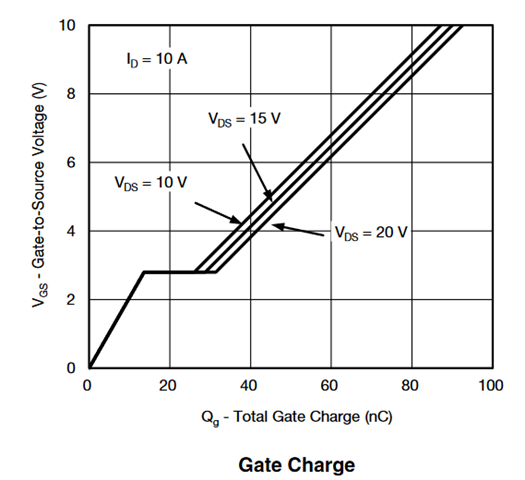
    The Qg of the FET should be taken at the nominal VCC voltage of the LM25085. 135nC seems very high. The IC's current consumption just related to driving the FET is Ivcc = Qg*Fsw, and this should be less than the VCC current limit. Send on the FET part number if you need more support.

    The 22uF/35V cap is okay, but X7R is preferable to X5R (125degC vs. 85degC max). The voltage rating is high -- consider instead 22uF/25V for the 15V output and 47uF/10V for the 2V and 6V outputs. 2-4mOhm is a good estimate for the ESR (it is effectively insignificant).

    Regards,

    Tim

  • Hi Tim,

    If I consider 135nC, the VCC current limit is overloaded. The FET used is the SI7149ADP, as mentioned in the LM25085A_Quick_Start - 15V.xls file. Could you, please, confirm to me which Qg should I use? If we have to consider 135nC indeed, could you, please, suggest a compatible FET for this application?

    About the output caps, understood, thank you.

    In the previous reply, I asked about the difference between the inductors suggested by both the WEBENCH and the quick start calculator. Can I keep the inductors suggested by the WEBENCH, or do I need to change them?

    And, can I consider the LM5088 design OK?

    Thank you again, Tim.

    Best regards,

    Jorge

    SI7149ADP.pdf

  • Jorge,

    From the datasheet, the Qg of that FET at VCC = 7.7V is ~70nC

    Consider the SiR167DP (5mOhm, 55nC @ 7.7V) or Si7143DP (10mOhm, 35nC @ 7.7V) instead.

    In terms of the quickstart, choose the inductance to give 30-40% of ripple current based on the full-load rating for each circuit. Also, enter the derated value for ceramic considering the voltage applied.

    Regards,

    Tim

  • Hi Tim,

    Thank you for your reply, and I am sorry for my late one.

    I changed the switching frequency of all the 4 power supplies to 300kHz, and I was based on the LM25085A_Quick_Start spreadsheet for the LM25085A controllers. Actually, I should have done this since the beginning.

    I have considered 20% of the output current to determine the inductor ripple current.

    Could you, please, evaluate again the 4 power supplies (1x LM5088 and 3x LM25085A) and give me an "OK" if you agree with them so that I can start the layout?

    The schematics and the spreadsheets are attached.

    Thanks again for your attention.

    Best regards,

    Jorge

    7041.LM25085A_Quick_Start - 15V.xls3652.LM25085A_Quick_Start - 6V.xls6318.LM25085A_Quick_Start - 2V.xls

  • Thanks, Jorge. I'll take a look shortly.

    If you would prefer a smaller inductor, 30-40% ripple current is acceptable and typically provides a better copper loss / core loss balance.

    Regards,

    Tim

  • Hi Tim,

    I think I will keep the inductors based on 20% of the output current... I noted that the LM25085A_Quick_Start spreadsheet uses this parameter, so I decided to use this as a default for all of the 4 power supplies.

    When you have some news regarding the analises, just let me know.

    Thanks Tim.

    Best regards,

    Jorge

  • Thanks, Jorge. I will take a look and get back to you tomorrow.

    Regards,

    Tim

  • Hi Tim,

    Were you able to check the designs?

    Best regards,

    Jorge

  • Hi Jorge - sorry I was backed up the last few days - I will review it tonight and get back to you.

    Regards,

    Tim

  • Hi Tim,

    Sorry for ask again. But actually I have finished the layout and I just would like an "OK" from you regarding the schematic. I really think it is OK now, it is just for warranty...

    Thanks, Tim.

    Best regards,

    Jorge

  • Hi Jorge,

    For the LM25085 schematics, there's a diode in series with the FET of one of the designs - maybe you can confirm why that's needed. Also, one of the output caps has a 12 Ohm series resistor, which isn't required when a type-3 ripple injection is installed.

    For the LM5088 IBB design, you have a cap from VIN to -VOUT near the FETs, so that provides all the high-frequency current and reduces the power loop parasitic inductance. Maybe make this value higher than the existing 1uF. Also 150k/390pF puts a zero at 2.7kHz, which is fine, but 150k implies a high gain, so check the loop crossover when you have the circuit up and running.

    Regards,

    Tim

  • Hi Tim,

    Thank you for your comments.

    The +6V power supply is used to store and supply energy after the power down during some time, 4 or 5 seconds. The diode D201 was inserted there so that the current doesn't flow from the capacitor C220 (1F/9V) to the +24V circuitry. The resistor R209 (12 Ohm) is used to charge the capacitor slowly, avoiding inrush current in the +6V power supply.

    About the LM5088 IBB design, I changed the capacitor C107 (1uF) to 22uF. I will check the circuit's behavior using the 150kOhm/390pF components.

    I think everything is clear now. If you have some concern about the diode D201 used in the +6V power supply, please let me know. If it is OK, please, let me know too, then I will finish the ticket.

    Thanks a lot for all your support until now, Tim.

    Best regards,

    Jorge.

  • Sounds good, Jorge. The diode could be at the actual input (not between the FET and shunt).

    Regards,

    Tim