This thread has been locked.

If you have a related question, please click the "Ask a related question" button in the top right corner. The newly created question will be automatically linked to this question.

LM2623-Q1: LM2623-Q1 Switching frequency

Part Number: LM2623-Q1
Other Parts Discussed in Thread: TPS61089, LMR62014, TPS61170

Hi,

I am currently using the LM2623-Q1 in one of my design with the following requirements:

- Vin [6;8.4V]

- Vout 12V

- Load: <= 0.4A

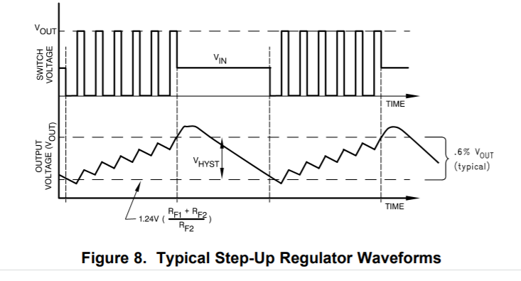
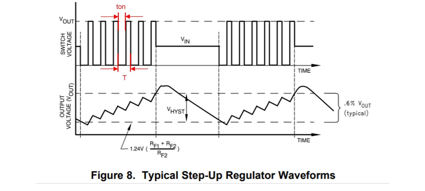
I followed the reference design but the capacitor C3 is a bit tricky to select. I removed it so it uses the default 17% duty cycle to application note AN-1221.

Selecting the correct resistor R3 is also tricky since the datasheet only shows input voltage up to 4.2V. I went for a 200k resistor.

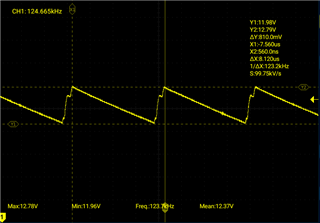
RF1 is 866k and RF2 is 100k, this should in theory lead to an output voltage of 11.978V

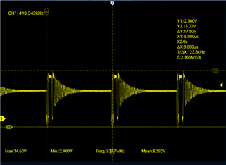
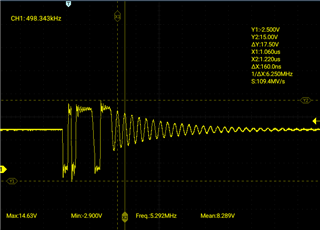
In practice I observe an output that indeed reaches 11.98V min, but with a swing up to 12.6V. I also see that the switching frequency is very low, around 140kHz.

The ripple would surely be less with a higher switching frequency but I don't understand how to increase it. I tried decreasing R3 value with no beneficial effect.

Below is the schematic (not that the reference designators do not match the datasheet, sorry about that)

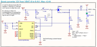
Thanks in advance for your help

  • HI Marc,

    If possible, please select TI newer boost converter TPS61089, LMR62014, TPS61170. These devices are cheaper and easy-to-use.

    For R3, C3 selection, choosing the correct C3 capacitor to obtain the appropriate duty cycle for a particular application circuit is a trial-and-error process. The non-linear effect that C3 produces is dependent on the input voltage and output voltage values. The correct C3 capacitor for specific input and output voltage values cannot be calculated. Choosing the correct C3 capacitance is best done by trial and error.

  • Hi Zack,

    I will definitely select another boost converter for the next iteration.

    Your answer only concerns the duty cycle (that's a quote from the datasheet), for it doesn't explain why the switching frequency is so low.

    The datasheet says for R3:

    The switching frequency of the oscillator is selected by choosing an external resistor (R3) connected between VIN
    and the FREQ pin. See Figure 3 in the Typical Characteristics for choosing the R3 value to achieve the desired
    switching frequency. A high switching frequency allows the use of very small surface mount inductors and
    capacitors and results in a very small solution size. TI recommends a switching frequency between 300 kHz and
    2 MHz

    The switching frequency I get is twice as low as the lowest recommended setting with a 200kOhm resistor and the input voltage of 8.4V

  • Hi Marc,

    Could you measure the SW node waveform?

    Please note you might note measure the correct switching frequency. 

    LM2623-Q1 implements Gated Oscillator Control Scheme, the switching waveform is like PFM mode. You can read datasheet part 7.3.1, 7.3.2 for more information.

  • Hi Zack,

    No problem for the SW node scope screenshots. You will find them below.

    Pretty strong ringing on the SW pin.

    Ok I think I understand what you mean. But by increasing the switching frequency, does the off time of the switch voltage stays the same or gets shortened as well ?

    If not shortened, I guess my only solution to reduce the voltage swing is to reduce the duty cycle.

    Let me know what you think

  • Hi Marc,

    You could try to reduce the duty cycle or switching frequency so that the output voltage maybe more flat. 

    But you know in light load condition, the device will definitely work like the above waveform: switches for several cycles, then stops switching until Vout is less than target voltage.

  • Hi Zack,

    I figured I would have to modify duty cycle or switching frequency. Regarding your comment on light load condition, the problem is the device does not switch before  Vout is under target voltage. It switches back on before it gets under target voltage and the ripple is massive. On the 1st scope capture I provided it is 0.81V (6.1% of Vout), which is an order of magnitude above the approx "typical" 0.6% of Vout of the waveform provided in the datasheet.

    I tried changing the duty cycle and switching frequency according to the datasheet (R3 being used to change the switching frequency and C3 the duty cycle). But the behavior I get is absolutely not aligned with the datasheet.

    Typically, it is said that an increase of C3 capacity will result in an increase of the duty cycle. I got the following result with an R3 of 200kOhm:

    - C3 = 4.7pF --> Duty cycle = 3.6%

    -C3 = 1pF --> Duty cycle = 5.4%

    -C3 = 0 (removed) --> Duty cycle = 12.8%

    Changing R didn't help either. The "best" I got is with R3 = 200k and C3 = 0

    Zack, do you believe the swing would flatten a bit under heavier load ?

  • Hi Marc,

    For boost converter, the time that SW equals 0V means the main switch turns on. So the duty cyle = ton/T, shown as below waveform, which is different from buck converter. 

    Could you share the waveforms that with different C3?

    Another thing is: it's always required to place a ceramic capacitor at output side in parallel with the bulk capacitor. In you schematic, is the C7 an aluminum electrolytic capacitor? Did you have a ceramic capacitor on PCB? Maybe this is not the key point to help solve your large ripple issue. Just want to remind you.