


Hello
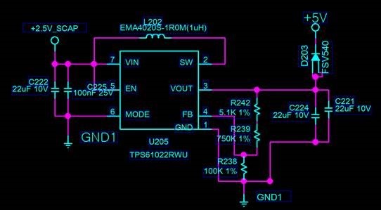
The SW pin was shorted to GND while testing the Supercapacitor backup power supply with the TPS61022 at the customer.
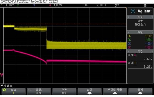
I have attached the circuit diagram and waveform, so please check it.
Yello : VOUT
Red : Vin
Best regards.
Hello
The SW pin was shorted to GND while testing the Supercapacitor backup power supply with the TPS61022 at the customer.
I have attached the circuit diagram and waveform, so please check it.
Yello : VOUT
Red : Vin
Best regards.

