This thread has been locked.

If you have a related question, please click the "Ask a related question" button in the top right corner. The newly created question will be automatically linked to this question.

TPS63000: Separate VIN and VINA supplies (VINA > VIN)

Part Number: TPS63000
Other Parts Discussed in Thread: TPS630242, TPS63030

Hi, 

I was looking at the TPS63000 datasheet and noticed the split VIN and VINA pins, and wondered if VIN and VINA could have different voltage supplies, i.e. VINA > VIN.

I have seen a previously resolved post on this forum regarding the TPS630242, however the question asked there was what happens when VINA < VIN. 

Some background. I am looking to connect VIN to a solar panel, and use the TPS63000 to charge a battery. The idea was that perhaps, if the control stage (VINA) can be supplied by the 2.5V+ battery, the power stage (VIN) might continue regulation below the recommended minimum 1.8V input voltage, and the battery would continue charging at lower solar panel input voltages.

Thanks in advance.

  • Hi  Boland,

    sorry to tell you that is not allowed for devise may damaged for high difference voltage between them.

    Regards

    Tao

  • Hi Tao, thank you very much for your reply.

    Are you able to expand a bit?

    How exactly will this damage the board seeing as the control and power stage appear separated in the block diagram. Or is it just operating outside of the recommended range so cannot advise to use it under these conditions? What do you define as a "high difference in voltage"?

    I guess another question is why is this not mentioned in more detail in the datasheet and should the pins not be internally tied together to avoid the user damaging the IC?

    Thanks again!

  • Hi  Boland,

    my apologize, i did not watch your question carefully and i take TPS63000 as other device,such like TPS63030(VIN and VINA connected via some components internally).

    my concern is when voltage of VINA is much higer than voltage of VIN which means "high difference in voltage", the internal components will be damaged, may be you can treat this components as a high Rdson FET.

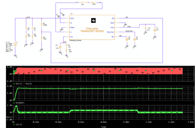
    For TPS63000, it is ok when voltage of VINA is higer than VIN, it will work normally in simulation. see picture bellow

    but make sure Vin always higher than 1.9V, or else it will fail to start-up.

    Regards

    Tao

  • Hi Tao, 

    What is the reason for the minimum input voltage? Is this the Vgs threshold voltage of the power stage transistors?

    Regards

  • Hi Boland,

    actually, i am not sure minimum input voltage is decided by what. but it should not be the Vth of FET, Vth of FET can be smaller. may be depend on some logic module and i am not sure which one.

    Regards

    Tao

  • Hi Tao,

    OK, thanks. I do not see in the block diagram that there are any logic modules supplied by VIN but of course that is not a complete representation of the full system. Who do I need to ask to find this information out?

    Regards

  • Hi  Boland,

    can you sent me a email? i think i need help from designer to answer your question and will loop you.

    Regards

    Tao