


Other Parts Discussed in Thread: TPS62816-Q1
Dear team:
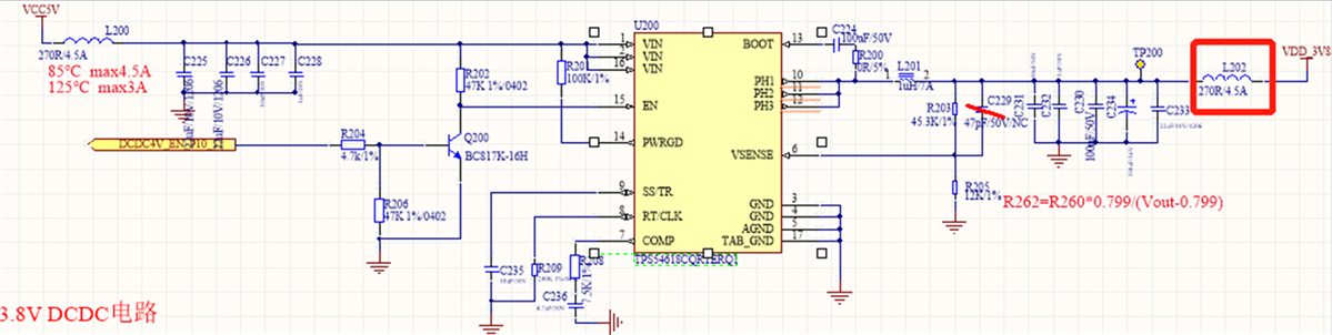
We recently used TPS54618CQRTERQ1 for 5V input and 3.8V output;
In the process of power optimization, the following two groups of tests were conducted when L202 in the figure-1 was disconnected, and the test data were recorded as follows:
Figure-1
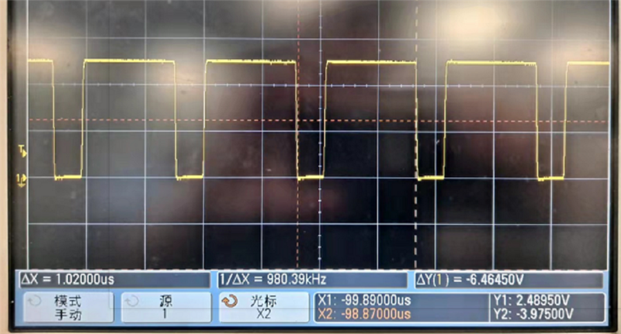
1. The first set of test records:
RT=200k;
1)Theoretical calculation:
FSW = 981 KHZ;
Duty ratio = 3.8/5 = 76%;
2)The actual measurement is as follows:
FSW = 1/1.02us = 980 KHZ;
Duty ratio = 0.8/1.02 = 78%;
Vsense = 0.799 V.
5V input current =10mA;
Figure-2
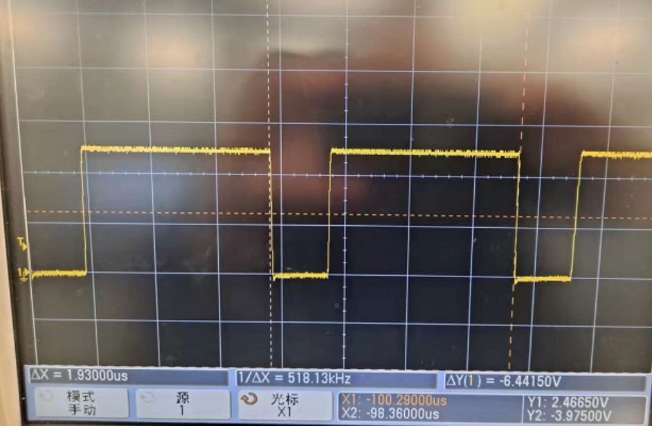
2. The second set of test records:
RT=390k
1)Theoretical calculation:
FSW = 512 KHZ;
Duty ratio = 3.8/5 = 76%;
2)The actual measurement is as follows:
FSW= 1/1.93 us = 518 KHZ;
Duty ratio = 1.465/1.93 = 75.9%;
Vsense = 0.799 V.
5V input current =14mA;
Figure-3
questions:
1. May I ask whether the measured power consumption of the chips in these two groups of test results is normal relative to the chip design?
2. Do you have test data for reference?
