Hi Team,
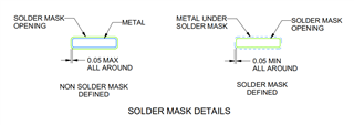
Download the latest specification from TI's official website and check the packaging suggestion as shown in Figure 1. The size of pin pad given in the packaging design is shown in Figure 2, and the size of solder resistance layer and tin plating layer of pin pad is shown in Figure 3.
Would like to ask:
1. How to determine the size of solder resistance layer and tin plating layer for IC pin design?
2. The phenomenon of tin connection between pins occurs in the process of SMT. Are there any suggestions for improvement in packaging?
Thank you very much!
Fig1.
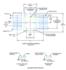
Fig 2
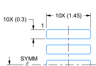
Fig3