This thread has been locked.

If you have a related question, please click the "Ask a related question" button in the top right corner. The newly created question will be automatically linked to this question.

TPS6521845: How to connect unused pins?

Part Number: TPS6521845
Other Parts Discussed in Thread: TPS65218

Some of the pins are not used in the design. How should they be connected: 

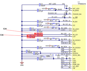
1. DCDC2 is not used in design. But PGOOD state depends on DCDC2 and PGOOD is used.

Would this be ok as DCDC2 connection ? (to save some PCB space)

  • connect IN_DCDC2 to VIN and omit the input capacitor
  • leave L2 output floating
  • connect FB2 to 3.3V from DCDC4 (directly or via voltage divider)
  • voltage on FB2 input would then satisfy PGOOD (overvoltage doesn’t matter as STRICT=0b and overvoltage is not monitored)

2. LS2, LS3 not used (TPS6521845 not configured via I2C in design)

  • connect IN_LS2, IN_LS3 to GND and leave outputs LS2-3 floating?

3. LS1 not used (but LS1 is enabled by sequence)

  • connect IN_LS1 to GND an leave output LS1 floating?
  • or connect IN_LS1 to voltage greater than 1.2 V ? (as LS1 is not disabled and 1.2 V is the minimum operating voltage for LS1)

4. LDO1 not used but PGOOD state depends on LDO1 and PGOOD is used.

  • connect IN_LDO1 to VIN and omit input and output capacitor
  • Hi Asko,

    Below are the recommended connections for the unused rails on TPS6521845 specifically if STRICT=0 (CONFIG1 register 0x13 / bit 2). This recommended connections will change if STRICT=1 or if you are using a different NVM config. 

    • DCDC2: FB2 needs can be tie to the feedback of another regulator with a higher output voltage and a lower Strobe (to make sure it is available before DCDC2). For example, if DCDC2 default is 1.425V, then FB2 can be connected to FB4 (assuming DCDC4 output voltage is higher than DCDC2). You can leave L2 floating. IN_DCDC2 should be connected to the same input voltage as IN_BIAS.  
    • LS2/LS3: These are disabled by default on the NVM config for TPS6521845 so you can leave both, inputs and outputs floating. 
    • LS1: IN_LS1 (input) should be connected to GND while LS1 (output) is left floating.
    • LDO1: IN_LDO should be tied to IN_BIAS and the output (LDO1) should be tied to a voltage higher than LDO1 default voltage (> 1.8V) that is available before the LDO1 powers up. 

    I also recommend validating this configuration using the TPS65218 BoosterPack (BOOSTXL-TPS65218)

    Thanks,

    Brenda

  • Thanks,

    A few questions more:

     Related to LS1 when not used…recommendation is to connect IN_LS1 (input) to GND and leave LS1 (output) floating.

    • is there risk that PMIC will give an interrupt due to grounded input as LS1 is enabled by sequencer?
    • datasheet specifies 1.2 V as minimum operating voltage for LS1, shouldn’t this be followed when LS1 is enabled?
    • any issue if IN_LS1 is connected to output of DCDC4 (3.3V) and LS1 (output) is left floating?

    Br, Asko

  • Hi Asko,

    If you get an interrupt on the INT2 register (address 0x12 / bit0), it can be cleared by disabling LS1 on the ENABLE2 register (address 0x12 / bit 1). This should not execute the power down sequence as the supervisor monitors DCDC1/2/3/4 and LDO1. Please let me now if you see any issues with this approach. I'm also adding a link to a previous E2E where this question was answered.  

    https://e2e.ti.com/support/power-management-group/power-management/f/power-management-forum/547376/tps65218---unused-load-switch-could-be-left-floating/2003736?tisearch=e2e-sitesearch&keymatch=tps65218%25252525252520LS1#2003736

    Thanks,

    Brenda

  • Hi and thanks a lot so far...

    One more detail to be clarified: What is TPS6521845 output voltage of DCDC1? In iMX6 application note (SLVAE94A) it is mentioned 1.35V. But in TPS6521845 datasheet it mention register value is 35h à 1.425V.

    Br, Asko

  • Hi Asko,

    The DCDC1 output voltage on TPS6521845 is 1.425V as stated in the datasheet. The i.MX 6Solo, 6DualLite application note (SLVAE94A) uses TPS6521815 which is the TPS65218 variant that comes with a "blank EEPROM" so customers can re-program the NVM to match the processor power requirements. 

    Thanks,

    Brenda

  • Hi again,

    The design is progressing, therefore still a question:

    • any issue if IN_LS1 is connected to the output of DCDC4 (3.3V) and LS1 (output) is left floating? This way interrupt is maybe avoided (We plan to use PMIC without SW support for now but nINT output is connected to the processor for future purposes. We want to avoid possible SW reaction to the interrupt. )

    Br, Asko

  • Hi Asko,

    I would have to check those connections with an EVM. Should be able to provide an update by end of the week. 

    Thanks,

    Brenda

  • Hi Asko,

    I removed the two capacitors connected to the load switch on the TPS65218 EVM and shorted the input (IN_LS1) to GND while keeping the output (LS1) floating. No issues were seen. I did not see any interrupt in the INT registers. If customer wants to use a different configuration, I would recommend verifying the connections on the EVM first before doing any implementation.   

    Thanks,

    Brenda

  • Thanks a lot, again

    The next one: The DCDC1 voltage of 1.425V is a bit undesired, and 1.35V could be better (less dissipation). Can the output voltage be tuned down by external feedback resistors?

    The DS did not tell anything about the possible usage of the resistors.


    Br,Asko

  • Hi Asko,

    The resistor divider is not needed on this PMIC. The TPS65218x is user programmable and the voltage for all rails can be changed through I2C. Additionally the new output voltage can be saved into the VNM so it becomes the new power-up default value. 

    Thanks,

    Brenda