This thread has been locked.

If you have a related question, please click the "Ask a related question" button in the top right corner. The newly created question will be automatically linked to this question.

BQ76PL455EVM: TMS57004 Launchpad

Part Number: BQ76PL455EVM
Other Parts Discussed in Thread: BQ76PL455A-Q1

Hi,

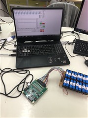
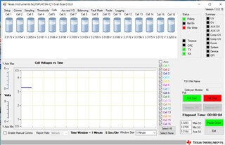
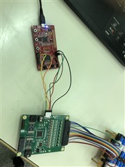
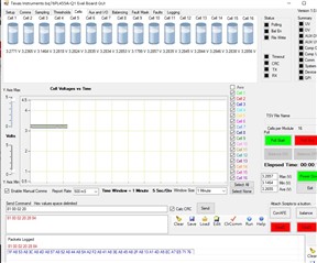
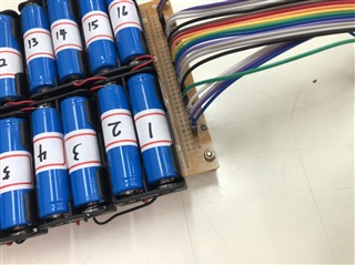
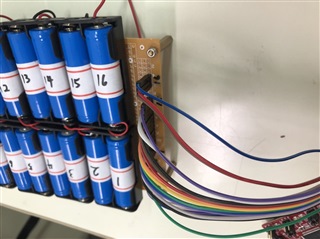
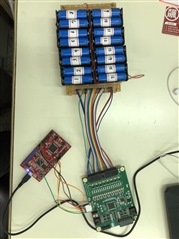
I am trying to program the TMS57004 Launchpad with the sample code provided by TI to work with the BQ76PL455EVM.

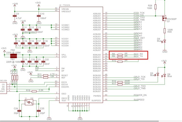
I see the "NOTE: Make sure that the resistor R8 is removed on the TMS570 Launchpad board." 

I have a question : I found that the circuit diagram R8 in the design document is 0 ohm. After removing it, the circuit is open, right?

If I remove the R8 in my TMS570 Launchpad , it can work regular when I use BQ76PL455EVM to connect TMS570 ?  or I should short circuit?

Could you tell me why should do that. 

Very Thanks.

  • Hello Kuanlei,

    Which document is making this recommendation? I agree that this doesn't make sense based on the schematic you are showing above. I suggest you try to communicate with the BQ device without depopulating this 0 ohm resistor first. 

  • Hi Alexander Scheuermann
    Thank for your reply!

    I found recommendation in http://www.ti.com/lit/pdf/slva617  page 4, 3.1 NOTE.

    When I use the USB to TTl cable. The BQ76PL455EVM works as expected right . Figure 1 show that.

                                                  Figure 1

    But,how do I know  it works normally when I use TMS57004 Launchpad with the sample code provided by TI to use it with BQ76PL455EVM.

    Now, I connect the MCU to the PC with USB cable ,and MCU jumper wires to the BQ76PL455EVM.,  then use CCS to run the sample code.Figure 2 show that, also can see the BQ Switch configuration in Figure 2.

                                               Figure 2

    Where could I see the cells voltage when the BQ Send data back to MCU?

    Very Thanks

  • Kuanlei,

    You should be able to send the read command for the cell voltage registers. Have you followed the steps in "2.1 Summary of Steps for Configuring AFE"?

  • Hi Alexander Scheuermann
    Thank for your reply!

    I follow the bq76PL455A-Q1 Software Design Reference 2.1 Summary of Steps for Configuring AFE.

    // Configure AFE (section 2.2.1)
    nDev_ID = 0;
    nRead = ReadReg(nDev_ID, 198, &sr_num, 2, 0); // 0ms timeout

    nDev_ID = 0;
    nSent = WriteReg(nDev_ID, 60, 0x00, 1, FRMWRT_SGL_NR); // set 0 mux delay
    nSent = WriteReg(nDev_ID, 61, 0x00, 1, FRMWRT_SGL_NR); // set 0 initial delay

    //Configure Voltage and Internal Sample Period( 2.2.2 )
    nDev_ID = 0;
    nSent = WriteReg(nDev_ID, 0x3E, 0xCC, 1, FRMWRT_SGL_NR); // set 99.92us ADC sampling period

    // Configure the Oversampling Rate(2.2.3 )
    nDev_ID = 0;
    nSent = WriteReg(nDev_ID, 7, 0xFC, 1, FRMWRT_SGL_NR); // CMD_OVS_CYCLE = 1; CMD_OVS_HPER = 3; CMD_OVS_GPER = 3; CMD_OVSMP = 4

    // clear fault and check ( 2.2.4 )
    nDev_ID = 0;
    nSent = WriteReg(nDev_ID, 81, 0x38, 1, FRMWRT_SGL_NR); // clear fault flags in the system status register
    nSent = WriteReg(nDev_ID, 82, 0xFFC0, 2, FRMWRT_SGL_NR); // clear all fault summary flags


    nDev_ID = 0;
    nSent = WriteReg(nDev_ID, 0x0E, 0xD2, 1, FRMWRT_SGL_NR); // Configure Device


    nDev_ID = 0;
    nSent = WriteReg(nDev_ID, 0x0F, 0x80, 1, FRMWRT_SGL_NR); // Configure Power
    nSent = WriteReg(nDev_ID, 0x10, 0x1080, 2, FRMWRT_SGL_NR); // Communication configuration

    And follow 4.2 Detailed Steps for Reading Voltages from Single Board in Daisy-Chain Network.

    Where can I see the Voltages in the CCS ?

    I probably know the Voltages data are in the bFrame right?

    // Send sample request to single board to sample and send results (section 4.2)
    nDev_ID = 0;
    nSent = WriteReg(nDev_ID, 2, 0x01, 1, FRMWRT_SGL_NR); // send sync sample command
    nSent = WaitRespFrame(bFrame, 27, 0); // 24 bytes data + packet header + CRC, 0ms timeout

  • Hello Kuanlei,

    I don't see a read command in your code. Are you reading the cell voltages at all?

    455 Datasheet text that may be helpful:

    7.6.3.2 CMD 0x02 (2) Command

    Write_With_Response requests directly targeted to this register cause the specified command to execute and the

    corresponding results to return a response. The number of bytes returned will be based on the bits selected in

    the CHANNELS register. Some bits in the CHANNELS register have more than one value returned, refer to their

    descriptions under the CHANNELS register.

    NOTE

    This transaction will return results from the command, not a read of register values.

    It is not possible to read the last value written to this register. Indirect reads of this register produce an undefined

    value for this register.

    A command sent to this register without writing the CHANNELS or OVERSMPL registers in the same frame uses

    the values currently in those registers. If a command writes the CHANNELS or OVERSMPL registers in the same

    frame then sends the command to the register, the new register values will overwrite the current register values

    and the execution of the command uses the new values.

    Requested values return MSB first in the order that they exist in the CHANNELS register, starting with the MSB

    (Cell 16, Cell 15 …). No values return for bits not selected in the CHANNELS register.

  • Hi Alexander Scheuermann
    Thank for your reply!

    The read command is  Software Design Reference section 3.3.2 ?

    // Read sampled data from boards (section 3.3.2)
    // 24 bytes - still configured for 8 AFE channels plus 2 AUX channels plus internal digital and analog die
    // temperatures (see code for section 2.2.5.2)
    nDev_ID = 0;
    nSent = WriteReg(nDev_ID, 2, 0x20, 1, FRMWRT_SGL_R); // send read sampled values command
    nSent = WaitRespFrame(bFrame, 27, 0); // 24 bytes data + packet header + CRC, 0ms timeout

    // Send sample request to single board to sample and send results (section 4.2)
    nDev_ID = 0;
    nSent = WriteReg(nDev_ID, 2, 0x01, 1, FRMWRT_SGL_NR); // send sync sample command
    nSent = WaitRespFrame(bFrame, 27, 0); // 24 bytes data + packet header + CRC, 0ms timeout

  • Hello Kuanlei,

    Yes, that's correct.

  • Hi Alexander Scheuermann
    Thank for your reply!

    When I read command set up finish.

    How could I see the response for  channel  data in CCS?

    I set the bFrame in the Expressions,but it didn't found.

    When I used the GUI it can response correct data.

  • Kuanlei,

    How are you monitoring for the returned data? The command looks correct, but I don't see where you are receiving the data back. Shouldn't you be including some type of print statement to see the data in CCS?

    Otherwise, are you configuring the registers for which cells need to be read back? Which cells are you expecting data from?

    I apologize for my limited software experience.

  • Hi Alexander Scheuermann
    Thank for your reply!

    I set the bFrame in the watch window but almost value is 0

    I set the read command and set the Interrupt to the bFrame 

    The hardware part I put the 4 0S wires in the same com & 3 16S wires in the same com & 1~16 wires in sequence.

    Is it connect correct? 

  • This is my hardware pictures.

  • This is my all code

    /**
     *
     *  @file main.c
     *  @brief this file contains example command sequences and functions to interface with the bq76PL455A-Q1 from a
     *  microcontroller. The examples provided are described in the bq76PL455A-Q1 Software Design Reference (SLVA617A)
     *  and the sections that correlate to each example are noted in the comments.
     *
     *  This code was written for the TMS570LS04x Launchpad Board, modified to remove R8, allowing use of the SCI1 UART.
     *  A bq76PL455A-Q1 EVM single-ended communication interface is connected to the Booster pack connectors J1 and J2 as
     *  shown below. Connection of these boards must be made by the user.
     *
     *  J1 pin 1 (+3V3)     -> bq76PL455A-Q1 EVM J3 pin 3 (VIO)
     *  J1 pin 3 (SCI1_RX)  -> bq76PL455A-Q1 EVM J3 pin 5 (TX) **remove R8 from TMS570LS04x Launchpad
     *  J1 pin 4 (SCI1_TX)  -> bq76PL455A-Q1 EVM J3 pin 4 (RX)
     *  J2 pin 1 (GND)      -> bq76PL455A-Q1 EVM J3 pin 1 (DGND)
     *  J2 pin 3 (GIOA0)    -> bq76PL455A-Q1 EVM J3 pin 6 (nWAKE)
     *  J2 pin 4 (GIOA1)    -> bq76PL455A-Q1 EVM J3 pin 2 (nFAULT)
     *
     *
     *
     *  @author Stephen Holland - Texas Instruments, Inc
     *  @date June 2015
     *  @version 1.0 Initial version
     *  @note Built with CCS for Hercules Version: 5.5.0
     */
    
    /*****************************************************************************
     **
     **  Copyright (c) 2011-2015 Texas Instruments
     **
     ******************************************************************************/
    
    /* USER CODE BEGIN (0) */
    /* USER CODE END */
    
    /* Include Files */
    #include "stdio.h"
    #include "sys_common.h"
    #include "system.h"
    
    /* USER CODE BEGIN (1) */
    #include "gio.h"
    #include "sci.h"
    #include "rti.h"
    #include "sys_vim.h"
    #include "swi_util.h"
    #include "crc.h"
    #include "pl455.h"
    #include "adc.h"
    
    int UART_RX_RDY = 0;
    int RTI_TIMEOUT = 0;
    
    /* USER CODE END */
    
    /** @fn void main(void)
     *   @brief Application main function
     *   @note This function is empty by default.
     *
     *   This function is called after startup.
     *   The user can use this function to implement the application.
     */
    
    /* USER CODE BEGIN (2) */
    /* USER CODE END */
    
    void main(void)
    {
        /* USER CODE BEGIN (3) */
    
        systemInit();
        gioInit();
        sciInit();
        sciSetBaudrate(scilinREG, BAUDRATE);
        rtiInit();
        vimInit();
    
        _enable_IRQ();
    
        WakePL455();
    
        CommClear();
    
        CommReset();
    
    
        // initialize local variables
        int nSent;
        int nRead;
        int nTopFound = 0;
        int nDev_ID;
        //int nGrp_ID;
        BYTE bFrame[132];
        uint32 sr_num, Dev_id, FLT_summ, FLT_UV, FLT_OV, FLT_COMUV, FLT_COMOV, FLT_OPCTR = 0;
    
        /** Code examples
         * The command sequences below are examples of the message examples in the bq76PL455 Communication Examples document.
         * each message example references the section in the document.
         */
    
    
        // Wake all devices
        // The wake tone will awaken any device that is already in shutdown and the pwrdown will shutdown any device
        // that is already awake. The least number of times to sequence wake and pwrdown will be half the number of
        // boards to cover the worst case combination of boards already awake or shutdown.
        for (nDev_ID = 0; nDev_ID < TOTALBOARDS; nDev_ID++)
        {
            nSent = WriteReg(nDev_ID, 12, 0x40, 1, FRMWRT_ALL_NR); // send out broadcast pwrdown command
            delayms(5); //~5ms
            WakePL455();
            delayms(5); //~5ms
        }
    
        // Mask Customer Checksum Fault bit
        nSent = WriteReg(0, 107, 0x8000, 2, FRMWRT_ALL_NR); // clear all fault summary flags
    
        // Clear all faults
        nSent = WriteReg(0, 82, 0xFFC0, 2, FRMWRT_ALL_NR); // clear all fault summary flags
        nSent = WriteReg(0, 81, 0x38, 1, FRMWRT_ALL_NR); // clear fault flags in the system status register
    
        // Auto-address all boards (section 1.2.2)
        nSent = WriteReg(0, 14, 0x19, 1, FRMWRT_ALL_NR); // set auto-address mode on all boards
        nSent = WriteReg(0, 12, 0x08, 1, FRMWRT_ALL_NR); // enter auto address mode on all boards, the next write to this ID will be its address
    
        // Set addresses for all boards in daisy-chain (section 1.2.3)
        for (nDev_ID = 0; nDev_ID < TOTALBOARDS; nDev_ID++)
        {
            nSent = WriteReg(nDev_ID, 10, nDev_ID, 1, FRMWRT_ALL_NR); // send address to each board
            nRead = ReadReg(nDev_ID, 10, &Dev_id, 1, 0); // 0ms timeout
        }
    
    //  Enable all communication interfaces on all boards in the stack (section 1.2.1)
        nSent = WriteReg(0, 16, 0x1080, 2, FRMWRT_ALL_NR); // 設置通信波特率並啟用堆棧中所有板上的所有接口
    
    
        /* Change to final baud rate used in the application (set by BAUDRATE define in pl455.h).
         * Up to this point, all communication is at 250Kb, as the COMM_RESET done at the initial
         * startup resets the bq76PL455A-Q1 UART to 250Kb. */
        switch (BAUDRATE)
                  {
                  case 125000:
                      nSent = WriteReg(0, 16, 0x00F8, 2, FRMWRT_ALL_NR); // set communications baud rate and enable all interfaces
                      delayms(1);
                      sciSetBaudrate(scilinREG, BAUDRATE);
                      break;
                  case 250000:
                      delayms(1);
                      break;
                  case 500000:
                      nSent = WriteReg(0, 16, 0x20F8, 2, FRMWRT_ALL_NR); // set communications baud rate and enable all interfaces
                      delayms(1);
                      sciSetBaudrate(scilinREG, BAUDRATE);
                      break;
                  case 1000000:
                      nSent = WriteReg(0, 16, 0x30F8, 2, FRMWRT_ALL_NR); // set communications baud rate and enable all interfaces
                      delayms(1);
                      sciSetBaudrate(scilinREG, BAUDRATE);
                      break;
                  case 9600000:
                      nSent = WriteReg(0, 16, 0x30F8, 2, FRMWRT_ALL_NR); // set communications baud rate and enable all interfaces
                      delayms(1);
                      sciSetBaudrate(scilinREG, BAUDRATE);
                      break;
                  }
    
                  /* Set communications interfaces appropriately for their position in the stack, and
                   * for baud rate used in the application (set by BAUDRATE define in pl455.h).
                   * (section 1.2.4)
                   */
                  for (nDev_ID = TOTALBOARDS - 1; nDev_ID >= 0; --nDev_ID)
                  {
                      // read device ID to see if there is a response
    
                      if (nRead == 0) // if nothing is read then this board doesn't exist
                          nTopFound = 0;
                      else // a response was received
                      {
                          if (nTopFound == 0)
                          { // if the last board was not present but this one is, this is the top board
                              if (nDev_ID == 0) // this is the only board
                              {
                                  switch (BAUDRATE)
                                  {
                                  case 125000:
                                      nSent = WriteReg(nDev_ID, 16, 0x0080, 2, FRMWRT_SGL_NR); // enable only single-end comm port on board
                                      break;
                                  case 250000:
                                      nSent = WriteReg(nDev_ID, 16, 0x1080, 2, FRMWRT_SGL_NR); // enable only single-end comm port on board
                                      break;
                                  case 500000:
                                      nSent = WriteReg(nDev_ID, 16, 0x2080, 2, FRMWRT_SGL_NR); // enable only single-end comm port on board
                                      break;
                                  case 1000000:
                                      nSent = WriteReg(nDev_ID, 16, 0x3080, 2, FRMWRT_SGL_NR); // enable only single-end comm port on board
                                      break;
                                  }
                              }
                              else // this is the top board of a stack (section 1.2.5)
                              {
                                  switch (BAUDRATE)
                                  {
                                  case 125000:
                                      nSent = WriteReg(nDev_ID, 16, 0x0028, 2, FRMWRT_SGL_NR); // enable only comm-low and fault-low for the top board
                                      break;
                                  case 250000:
                                      nSent = WriteReg(nDev_ID, 16, 0x1028, 2, FRMWRT_SGL_NR); // enable only comm-low and fault-low for the top board
                                      break;
                                  case 500000:
                                      nSent = WriteReg(nDev_ID, 16, 0x2028, 2, FRMWRT_SGL_NR); // enable only comm-low and fault-low for the top board
                                      break;
                                  case 1000000:
                                      nSent = WriteReg(nDev_ID, 16, 0x3028, 2, FRMWRT_SGL_NR); // enable only comm-low and fault-low for the top board
                                      break;
                                  }
                                  nTopFound = 1;
                              }
                          }
                          else // this is a middle or bottom board
                          {
                              if (nDev_ID == 0) // this is a bottom board of a stack (section 1.2.6)
                              {
                                  switch (BAUDRATE)
                                  {
                                  case 125000:
                                      nSent = WriteReg(nDev_ID, 16, 0x00D0, 2, FRMWRT_SGL_NR); // enable comm-high, fault-high and single-end comm port on bottom board
                                      break;
                                  case 250000:
                                      nSent = WriteReg(nDev_ID, 16, 0x10D0, 2, FRMWRT_SGL_NR); // enable comm-high, fault-high and single-end comm port on bottom board
                                      break;
                                  case 500000:
                                      nSent = WriteReg(nDev_ID, 16, 0x20D0, 2, FRMWRT_SGL_NR); // enable comm-high, fault-high and single-end comm port on bottom board
                                      break;
                                  case 1000000:
                                      nSent = WriteReg(nDev_ID, 16, 0x30D0, 2, FRMWRT_SGL_NR); // enable comm-high, fault-high and single-end comm port on bottom board
                                      break;
                                  }
                              }
                              else // this is a middle board
                              {
                                  switch (BAUDRATE)
                                  {
                                  case 125000:
                                      nSent = WriteReg(nDev_ID, 16, 0x0078, 2, FRMWRT_SGL_NR); // enable comm-high, fault-high, comm-low and fault-low on all middle boards
                                      break;
                                  case 250000:
                                      nSent = WriteReg(nDev_ID, 16, 0x1078, 2, FRMWRT_SGL_NR); // enable comm-high, fault-high, comm-low and fault-low on all middle boards
                                      break;
                                  case 500000:
                                      nSent = WriteReg(nDev_ID, 16, 0x2078, 2, FRMWRT_SGL_NR); // enable comm-high, fault-high, comm-low and fault-low on all middle boards
                                      break;
                                  case 1000000:
                                      nSent = WriteReg(nDev_ID, 16, 0x3078, 2, FRMWRT_SGL_NR); // enable comm-high, fault-high, comm-low and fault-low on all middle boards
                                      break;
                                  }
                              }
                          }
                      }
                  }
    
        // Configure AFE (section 2.2.1)
    
                  //讀出設備的序列號
                  nDev_ID = 0;
                  nRead = ReadReg(nDev_ID, 198, &sr_num, 2, 0); // 0ms timeout
    
                  nDev_ID = 0;
                  nSent = WriteReg(nDev_ID, 60, 0x00, 1, FRMWRT_SGL_NR); // set 0 mux delay
                  nSent = WriteReg(nDev_ID, 61, 0x00, 1, FRMWRT_SGL_NR); // set 0 initial delay
    
                  // 配置電壓和內部採樣週期(第 2.2.2 節)
                  nDev_ID = 0;
                  nSent = WriteReg(nDev_ID, 0x3E, 0xCC, 1, FRMWRT_SGL_NR); // set 99.92us ADC sampling period
    
                  // 配置過採樣率(2.2.3 節)
                  nDev_ID = 0;
                  nSent = WriteReg(nDev_ID, 7, 0xFC, 1, FRMWRT_SGL_NR); // CMD_OVS_CYCLE = 1; CMD_OVS_HPER = 3; CMD_OVS_GPER = 3; CMD_OVSMP = 4
    
                  // 清除並檢查故障(第 2.2.4 節)
                  nDev_ID = 0;
                  nSent = WriteReg(nDev_ID, 81, 0x38, 1, FRMWRT_SGL_NR); // clear fault flags in the system status register
                  nSent = WriteReg(nDev_ID, 82, 0xFFC0, 2, FRMWRT_SGL_NR); // clear all fault summary flags
    
                  // 設備配置
                  nDev_ID = 0;
                  nSent = WriteReg(nDev_ID, 0x0E, 0xD2, 1, FRMWRT_SGL_NR); // Configure Device
    
                  // 電源配置
                  nDev_ID = 0;
                  nSent = WriteReg(nDev_ID, 0x0F, 0x80, 1, FRMWRT_SGL_NR); // Configure Power
                  nSent = WriteReg(nDev_ID, 0x10, 0x1080, 2, FRMWRT_SGL_NR); // Communication configuration


        // Select number of cells and channels to sample (section 2.2.5.1)


      //nSent = WriteReg(0, 13, 0x10, 1, FRMWRT_SGL_NR);          // NCHAN : set number of cells to 16
        nSent = WriteReg(0, 13, 0x06, 1, FRMWRT_SGL_NR);          // NCHAN : set number of cells to 6
        nSent = WriteReg(0,  3, 0x000600C0, 4, FRMWRT_SGL_NR);     // select all cell, AUX channels 0 and 1, and internal digital die and internal analog die temperatures


        // Auto Monitor
        nDev_ID=0;
            nSent = WriteReg(nDev_ID, 50, 0x00, 1, FRMWRT_SGL_NR);          // Auto monitor period: Auto monitor off
     //     nSent = WriteReg(nDev_ID, 51, 0x003F0080, 4, FRMWRT_SGL_NR);    // Auto monitors channel select 1-6 cells
     //     nSent = WriteReg(nDev_ID, 55, 0xFB, 1, FRMWRT_SGL_NR);          // Sampling time 12.6 us and 8 samples are averaged
    
    
        // Thresholds Voltage settings
        nDev_ID=0;
        nSent = WriteReg(nDev_ID, 144, 0xCCCC, 2, FRMWRT_SGL_NR);       // set OV threshold = 4.000V
        /*  Threshold value is set like     5V      :   65535
         *                                  4.00    :   ?(X)
         *                                  X = (4.00 x 65535)/5
         *                                  X = 52428 DECIMAL
         *                                  Convert X to HEXADECIMAL
         *                                  X = CCCC
         */
        nDev_ID=0;
        nSent = WriteReg(nDev_ID, 142, 0x9999, 2, FRMWRT_SGL_NR);       // set UV threshold = 3.0000V
        /*  Threshold value is set like     5V      :   65535
         *                                  3.00    :   ?(X)
         *                                  X = (3.00 x 65535)/5
         *                                  X = 47185 DECIMAL
         *                                  Convert X to HEXADECIMAL
         *                                  X = B851
         */
        nDev_ID=0;
        nSent = WriteReg(nDev_ID, 140, 0x48, 1, FRMWRT_SGL_NR);         // set COMP_UV threshold = 2.500V
        /*
         *  Comp_UV threshold value is set like
         *  CMP_UV_THRES  :  These bits set the comparator undervoltage-threshold value in 25-mV steps. The range is determined
                             by the CMP_TST_SHF_UV bit.
         *  CMP_TST_SHF_UV : This bit sets the operating range for the undervoltage comparators.
                             0 = Normal range of 0.7 V to 3.875 V
                             1= Shifted range of 2.0 V to 5.175 V (used for self-test purposes)
            Here we will go for normal range of 0.7 V to 3.875 V. So, the actual range is 3.875 - 0.7 = 3.175
            Voltage value moves in the steps of 25mV. Therefore total steps  = 3.175/0.025 = 127 steps
            Let my COMP_UV threshold = 3.000V therefore steps = (3.00 - 0.7) / 0.025 =  92 steps
            Convert 92 into Hexadecimal : 0x5C
        */
        nDev_ID=0;
        nSent = WriteReg(nDev_ID, 141, 0x50, 1, FRMWRT_SGL_NR);         // set COMP_OV threshold = 4.000V
        /*
             *  Comp_OV threshold value is set like
             *  CMP_OV_THRES  :  These bits set the comparator Overvoltage-threshold value in 25-mV steps. The range is determined
                                 by the CMP_TST_SHF_UV bit.
             *  CMP_TST_SHF_OV : This bit sets the operating range for the undervoltage comparators.
                                 0 = Normal range of 2.0 V to 5.175 V
                                 1= Shifted range of 0.7 V to 3.875 V (used for self-test purposes).
                Here we will go for normal range of 2.0 V to 5.175 V. So, the actual range is 5.175 - 2.0 = 3.175
                Voltage value moves in the steps of 25mV. Therefore total steps  = 3.175/0.025 = 127 steps
                Let my COMP_UV threshold = 3.000V therefore steps = (4.00 - 2.00) / 0.025 =  80 steps
                Convert 80 into Hexadecimal : 0x50
            */
    
        // Cell Balancing
    
        nSent = WriteReg(nDev_ID, 19, 0x28, 1, FRMWRT_SGL_NR);          // General configuration for Balancing
        nSent = WriteReg(0, 30, 0x0005, 2, FRMWRT_SGL_NR);              //set BIST configuration (disable squeeze resistor)
        nSent = WriteReg(nDev_ID, 0x14, 0x003F, 2, FRMWRT_SGL_NR);        // Balance Enabling FETs
    
        // Faults
        nDev_ID = 0;
        nRead = ReadReg(nDev_ID, 82, &FLT_summ, 2, 0);                  // Fault summary
        nRead = ReadReg(nDev_ID, 84, &FLT_UV, 2, 0);                    // Fault_UV
        nRead = ReadReg(nDev_ID, 86, &FLT_OV, 2, 0);                    // Fault_OV
        nRead = ReadReg(nDev_ID, 90, &FLT_COMUV, 2, 0);                 // Fault_Comparator undervoltage
        nRead = ReadReg(nDev_ID, 92, &FLT_COMOV, 2, 0);                 // Fault_Comparator Overvoltage
        nSent = WriteReg(nDev_ID, 110, 0xFFC0, 2, FRMWRT_SGL_NR);       // Fault_Output control
        nRead = ReadReg(nDev_ID, 110, &FLT_OPCTR, 2, 0);                // Fault_Output control
        nRead = ReadReg(nDev_ID, 110, &FLT_OPCTR, 2, 0);                // Device Status
    
        // Configure GPIO pin direction and set new pin values (section 5.2.1)
                nDev_ID = 0;
                nSent = WriteReg(nDev_ID, 120, 0x07, 1, FRMWRT_SGL_NR); // set GPIO[2:0] to output direction
    
        // Configure AUX0 port with UV and OV
                nSent = WriteReg(nDev_ID, 146, 0x6674, 2, FRMWRT_SGL_NR);     // AUX0 UV threshold = 2V
                nSent = WriteReg(nDev_ID, 148, 0xCCE8, 2, FRMWRT_SGL_NR);     // AUX0 OV threshold = 4V
    
    
        if(FLT_summ != 0x00)
        {
            nSent = WriteReg(nDev_ID, 121, 0x07, 1, FRMWRT_SGL_NR); // set GPIO outputs (pattern b111)
        }
    
        if (!gioGetBit(gioPORTA, 1))
        {
            gioSetBit(gioPORTA, 2, 1); // GIOA2 (active high)
            delayms(1000);
            gioToggleBit(gioPORTA, 2); // GIOA2 ()
        }
    /*
     * ** nFault pin of BQ76PL455 is connected to TMS570 pin GIOA1. So when there is fault in the BQ76PL455,
     *    nFault pin becomes Active low and
     *    GIOA1 also goes low. So logic is like, if GIOA1 = 0, GIOA2 Led should turn ON, wait for 1000ms and then go OFF.
     */


      /*    nSent = WriteReg(nDev_ID, 122, 0x07, 1, FRMWRT_SGL_NR); // turn off GPIO[5:4] pull ups and turn on GPIO[2:0] pull ups
    
            nSent = WriteReg(nDev_ID, 121, 0x02, 1, FRMWRT_SGL_NR); // set GPIO outputs (pattern b010)
            nSent = WriteReg(nDev_ID, 121, 0x04, 1, FRMWRT_SGL_NR); // set GPIO outputs (pattern b100)
            nSent = WriteReg(nDev_ID, 121, 0x07, 1, FRMWRT_SGL_NR); // set GPIO outputs (pattern b111)
            nSent = WriteReg(nDev_ID, 121, 0x00, 1, FRMWRT_SGL_NR); // set GPIO outputs (pattern b000)
    */
        // Send sample request to single board to sample and send results (section 4.2)
    
          //nDev_ID = 0;
         // nSent = WriteReg(nDev_ID,0x02, 0x01, 1, FRMWRT_SGL_NR); // send sync sample command
        //  nSent = WaitRespFrame(bFrame, 27, 0); // 24 bytes data + packet header + CRC, 0ms timeout
    
        // Read sampled data from boards (section 3.3.2)
        // 24 bytes - still configured for 8 AFE channels plus 2 AUX channels plus internal digital and analog die
        // temperatures (see code for section 2.2.5.2)
    
        nDev_ID = 0;
        nSent = WriteReg(nDev_ID, 2, 0x20, 1, FRMWRT_SGL_R); // send read sampled values command
        nSent = WaitRespFrame(bFrame, 27, 0); // 24 bytes data + packet header + CRC, 0ms timeout
    
    
        /*  // Send sample request with embedded channel and oversample information (section 4.3.1)
         nDev_ID = 3;
         nSent = WriteReg(nDev_ID, 2, 0x0000FF03C000, 6, FRMWRT_SGL_NR); // send sync sample command with channel
         // selection and oversample selection embedded
         */
        // Read previously sampled data from single board (section 4.3.2)
       // nDev_ID = 0;
       // nSent = WriteReg(nDev_ID, 2, 0x20, 1, FRMWRT_SGL_R); // send read sampled values command
       // nSent = WaitRespFrame(bFrame, 27, 0); // 24 bytes data + packet header + CRC, 0ms timeout


        /*  // Configure GPIO inputs with or without pull ups or pull downs (section 5.2.2)
         nDev_ID = 0;
         nSent = WriteReg(nDev_ID, 123, 0x04, 1, FRMWRT_SGL_NR);    // enable pull down for GPIO2, turn off all other GPIO pull downs
         nSent = WriteReg(nDev_ID, 122, 0x03, 1, FRMWRT_SGL_NR);    // enable pull ups for GPIO[1:0], turn off all other GPIO pull ups
         nSent = WriteReg(0, 122, 0x03, 1, FRMWRT_ALL_NR);  // broadcast to all boards to enable pull ups for GPIO[1:0] and turn off all other GPIO pull ups
         */
        /*  // Setting a GPIO output value (section 5.2.3.1)
         nDev_ID = 0;
         nSent = WriteReg(nDev_ID, 120, 0x17, 1, FRMWRT_SGL_NR);    // set GPIO direction for GPIO4 and GPIO[2:0] as outputs, GPIO3 and GPIO5 as inputs
         nSent = WriteReg(nDev_ID, 121, 0x12, 1, FRMWRT_SGL_NR);    // set GPIO4 and GPIO1, clear GPIO2 and GPIO0
    
         // Reading a GPIO input value (section 5.2.3.2)
         nDev_ID = 0;
         nSent = WriteReg(nDev_ID, 120, 0x30, 1, FRMWRT_SGL_NR);    // set GPIO direction for GPIO[5:4] as outputs, GPIO[3:0] as inputs
         nRead = ReadReg(nDev_ID, 124, &wTemp, 1, 0);   // read GPIO inputs, 0ms timeout
         */
        /*  // Steps for saving register configuration to EEPROM (sections 6.2.1 to 6.2.4)
         // ** the code is commented out below to avoid accidental use - uncomment to use
         nDev_ID = 0;
         //nSent = WriteReg(nDev_ID, 130, 0x8C2DB194, 4, FRMWRT_SGL_NR);    // write Magic Number 1
         //nSent = WriteReg(nDev_ID, 252, 0xA375E60F, 4, FRMWRT_SGL_NR);    // write Magic Number 2
         //nSent = WriteReg(nDev_ID, 12, 0x10, 1, FRMWRT_SGL_NR);   // send Write RAM to EEPROM command
         nRead = ReadReg(nDev_ID, 12, &wTemp, 1, 0);    // read WRITE_EEPROM status bit, 0ms timeout
         //test WRITE_EEPROM bit to check for completion
    
         // Steps for saving register configuration to EEPROM in all devices in stack (sections 6.2.5)
         // ** the code is commented out below to avoid accidental use - uncomment to use
         //nSent = WriteReg(0, 130, 0x8C2DB194, 4, FRMWRT_ALL_NR);  // write Magic Number 1
         //nSent = WriteReg(0, 252, 0xA375E60F, 4, FRMWRT_ALL_NR);  // write Magic Number 2
         //nSent = WriteReg(0, 12, 0x10, 1, FRMWRT_ALL_NR); // send Write RAM to EEPROM command
         nDev_ID = 0;
         nRead = ReadReg(nDev_ID, 12, &wTemp, 1, 0);    // read WRITE_EEPROM status bit, 0ms timeout
         //test WRITE_EEPROM bit to check for completion
         nDev_ID = 1;
         nRead = ReadReg(nDev_ID, 12, &wTemp, 1, 0);    // read WRITE_EEPROM status bit, 0ms timeout
         //test WRITE_EEPROM bit to check for completion
         nDev_ID = 2;
         nRead = ReadReg(nDev_ID, 12, &wTemp, 1, 0);    // read WRITE_EEPROM status bit, 0ms timeout
         */ //test WRITE_EEPROM bit to check for completion
            // Assign devices to specific group IDs (section 7)
    /*    nDev_ID = 1;
        nSent = WriteReg(nDev_ID, 11, 0x01, 1, FRMWRT_SGL_NR); // assign Dev ID 1 to Group ID 1
        nDev_ID = 2;
        nSent = WriteReg(nDev_ID, 11, 0x01, 1, FRMWRT_SGL_NR); // assign Dev ID 1 to Group ID 1
    
        delayms(1);
    
    */
         // Send group sample request with embedded channel and oversample information (section 7.1)
         // send sync sample command (first data byte = command (b[7:5] = 0) | highest device to respond (0x01)) with
         // channel selection and oversample selection embedded
    /*     nGrp_ID = 1;
         nSent = WriteReg(nGrp_ID, 2, 0x02FFFF550000, 6, FRMWRT_GRP_R);
         nSent = WaitRespFrame(bFrame, 86, 0); // 40 bytes data (x2) + packet header (x2) + CRC (x2), 0ms timeout
    
         // Send group sample request - 1 byte method (section 7.2)
         // send sync sample command with channel (data byte = command (b[7:5] = 0) | highest device to respond (0x01))
         // sampling parameters are taken from values already stored in Command Channel Select and Oversampling registers
         nGrp_ID = 1;
         nSent = WriteReg(nGrp_ID, 2, 0x02, 1, FRMWRT_GRP_R);
         nSent = WaitRespFrame(bFrame, 86, 0); // 40 bytes data (x2) + packet header (x2) + CRC (x2), 0ms timeout
    
         // Send group register read - 2 byte method (section 7.3)
         // read Command Channel Select register (first data byte = highest device to respond (0x01), second data byte
         // = number of data bytes - 1 (4 bytes = 0x03))
         // sampling parameters are taken from values already stored in Command Channel Select and Oversampling registers
         nGrp_ID = 1;
         nSent = WriteReg(nGrp_ID, 3, 0x0203, 2, FRMWRT_GRP_R);
         nSent = WaitRespFrame(bFrame, 14, 0); // 4 bytes data (x2) + packet header (x2) + CRC (x2), 0ms timeout
    
         // Send group register read - 1 byte method (section 7.4)
         // read Command Channel Select register (data byte = number of data bytes - 1 (4 bytes = b011) | highest device
         // to respond (0x01))
         // sampling parameters are taken from values already stored in Command Channel Select and Oversampling registers
         nGrp_ID = 1;
         nSent = WriteReg(nGrp_ID, 3, 0x62, 1, FRMWRT_GRP_R);
         nSent = WaitRespFrame(bFrame, 14, 0); // 4 bytes data (x2) + packet header (x2) + CRC (x2), 0ms timeout
    
         // Send general broadcast register read - 2 byte method (section 8.1)
         // read Command Channel Select register (first data byte = highest device to respond (0x01), second data byte
         // = number of data bytes - 1 (0x03))
         nSent = WriteReg(0, 3, 0x0203, 2, FRMWRT_ALL_R);
         nSent = WaitRespFrame(bFrame, 14, 0); // 4 bytes data (x2) + packet header (x2) + CRC (x2), 0ms timeout
    
         // Send general broadcast register read - 1 byte method (section 8.2)
         // read Command Channel Select register (data byte = number of data bytes - 1 (4 bytes = b011) | highest device
         // to respond (0x01))
         nSent = WriteReg(0, 3, 0x62, 1, FRMWRT_ALL_R);
         nSent = WaitRespFrame(bFrame, 14, 0); // 4 bytes data (x2) + packet header (x2) + CRC (x2), 0ms timeout
    */
        while (1)
            ;
        /* USER CODE END */
    }
    
    /* USER CODE BEGIN (5) */
    /* USER CODE END */