


Other Parts Discussed in Thread: TPS62730
Hello All,
I would like to know what the most appropriate method is to create a BYPASS path for the TPS62136 buck converter? I would like to create a path where VCC is connected directly to the LOAD via a P-Channel MOSFET. I currently am thinking of 3 different MOSFET configurations for the BYPASS path. All 3 setups assumes that buck converter is Disabled (EN pin pulled LOW). I am not limited to the 3 setups that will presented here. I am open to other alternatives as well.
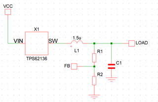
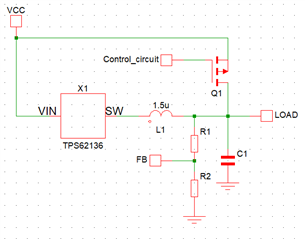
A. Single MOSFET after buck converter output.
Procedure to BYPASS: Buck IC EN pin pulled LOW and turn ON Q1
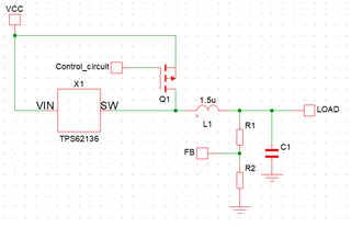
B. Single MOSFET before the inductor L1. I am basing this on the TPS62730 Buck IC that as an internal bypass FET
Procedure to BYPASS: Buck IC EN pin pulled LOW and turn ON Q1
For the first two methods, are there any concerns a reverse feedback current going inside back to the SW pin of the buck IC even if the EN pin is pulled low? Is the single MOSFET and disabled EN pin good enough to prevent any reverse currents? Should I place another MOSFET at the output of the buck converter to create a break in the circuit if Q1 is ON. This is the third setup I am considering
C. Two MOSFETS.
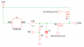
Q1 is the bypass MOSFET to connect VCC to the LOAD
Q2 is the MOSFET in-line with the buck converter
Procedure to BYPASS: Buck IC EN pin pulled LOW and turn OFF Q2 and turn ON Q1
1. Which of the three methods do you recommended to use?
2. What are other alternative methods for bypassing the Buck Converter to give the full VCC voltage to the LOAD, with minimum voltage drop?
Thank you!
