This thread has been locked.

If you have a related question, please click the "Ask a related question" button in the top right corner. The newly created question will be automatically linked to this question.

TPS1H000-Q1: GND connection when using GND Network

Part Number: TPS1H000-Q1
Other Parts Discussed in Thread: TPS1H100-Q1

Hi team,

Can I ask some questions about TPS1H000-Q1?

-. When using GND network (1Kohm // diode), which GND should DELAY pin be connected? device GND pin or System GND? 

-. TPS1H100-Q1 datasheet states the following sentence. Can you give some details why it may damage HSD or diode when inductive load is switching off?

"Type 3 (resistor and diode in parallel (recommended)): A peak negative spike may occur when the
inductive load is switching off, which may damage the HSD or the diode. So, TI recommends a resistor in
parallel with the diode when driving an inductive load. The recommended selection are 1-kΩ resistor in
parallel with an IF > 100-mA diode. If multiple high-side switches are used, the resistor and diode can be
shared among devices."

Thanks,

Sam Lee

  • Hi Sam,

    1. The Delay capacitor must be connected to IC GND.

    2. During inductive turn off, there will be a large negative spike on output of the device. Because of internal connection within the device, this can result in a large reverse voltage across the GND diode. If the diode is not rated for these reverse voltages (same magnitude as the negative spike) then the diode can be damaged. As such, a resistor in parallel provides a high impedance path for this event and thereby circumventing this issue while keeping any instantaneous reverse current flow very low.

    On the EVM we have used a input diode to protect against reverse voltage events. This is because the switch is for lower currents. I would also recommend this approach if possible in your system.

    Thanks,

    Shreyas

  • Hi Shreyas,

    Thank you for your answer. Can I ask one more quesion?

    When using input blocking diode instead of GND network, can it protect IC against inductive load(relay: about 150mA) switching off? I need your confimation.

    Thanks,

    Sam Lee

  • Hi Sam,

    The input diode and the Ground diode are all methods of protecting against the reverse current.

    To protect against the inductive spike, the device has an integrated V_ds clamp that keeps the conduction path active so as to dissipate the inductive energy.

    Thanks,

    Shreyas

  • Hi Shreyas,

    Thank you for your clarification. I thought that the GND network (resistor//diode) also would help protect the large negative spike during the inductive turn off, based on your previous comment. But, it's not that much helpful, compared to V_ds clamp, correct?

    Do you think that for the relay load (max 150mA) it's enought with the internal V_ds clamp without adding an external component(freewheel diode) to protect the switing off?

    Thanks,

    Sam Lee

  • Hi Sam,

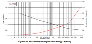
    In general, this depends on the magnetization energy in the inductance. At 150mA, the magnetization energy will be quite low.

    TPS1H100-Q1 will have no issues driving this and demagnetizing this load.

    Please refer to figure 34 on the datasheet as this describes the demagnetization capability of TPS1H100-Q1:

    Thanks,

    Shreyas

  • Hi Shreyas,

    Thank you for your comment.

    Can you provide the graph of TPS1H000-Q1 which we're actually using?

    Thanks,

    Sam Lee

  • Hi Sam,

    We do not have a graph to provide for TPS1H000-Q1 at this time.

    We do have one for TPS4H000 which is the four channel version of the device with 1mOhm on resistance.

    As you can see, 0.15A is a very low current and the supportable inductances are large.

    Thanks,

    Shreyas

  • Hi Shreyas,

    Thank you for your support.

    Best Regards,

    Sam Lee