This thread has been locked.

If you have a related question, please click the "Ask a related question" button in the top right corner. The newly created question will be automatically linked to this question.

UCC21520: UCC21520 vs UCC21540

Part Number: UCC21520
Other Parts Discussed in Thread: UCC21540,

Hi Team,

There is a good new that we could DIN TI product!

Customer have questions about UCC21520 and UCC21540.
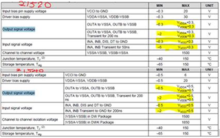
In the preliminary comparison, there is a difference between -0.3v and -0.5v in Output signal voltage! Why?
Is UCC21520 more stringent?
As far as I saw from SPEC, it’s a Pin to Pin IC.
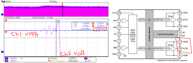
Rise/Fall time doesn’t seem to be difference
I want to know what are the other differences between UCC21520 and UCC21540? THX

  • Hello Kygo,

    Thanks for reaching out on E2E.

    UCC21540 is a newer version the UCC21520, with the main differences being the maximum voltages. UCC21520 can support up to 25V Output side VDD, while UCC21540 can only support 18V. On the primary side, UCC21520 can handle up to to 18V, but the UCC21540 can only support up to 5.5V. 

    However, the UCC21540 only has a power up delay of 40us, while UCC21520 has a delay of 50us.

    The difference in absolute minimum OUT voltage is a result of different silicon.

    In general, we recommend  UCC21540 unless VCCI is greater than 5.5V, or VDD is greater than 18V.

    Please let me know if we can help more, or click the green button if this answers your question.

    Regards,

    Daniel

  • Hi Daniel,

    Thank you for  your help

    May I know why UCC21540 & UCC21520 Maximum Ratings is deference?

    Cause UCC21540 : output signal voltage is VDD+0.5

    But UCC21520  : output signal voltage is VDD+0.3

  • Hi Kygo,

    UCC21540 is a newer part with a slightly different silicon design than UCC21520, leading to this difference in Output Abs Max.

    Is there a particular reason spec is important for your design? 

    Regards,

    Daniel

  • Hi Daniel,

    After discuss with customer ,one thing need you check

    We got the waveform VDDB & VOB High level 0.736V during 3.2ns as below picture! 

    As I know UCC21540 High_level over is VDDB+0.5V, like the waveform measured below, does it exceed  UCC21540 specifications? THX

  • Hi Kygo,

    For such a short duration this peak is not likely to damage the driver. That said, it would be better to keep this peak below the datasheet value of VDD +0.5V. This could be accomplished by: 1. Adjusting Rgate to reduce ringing. 2. reducing parasitic inductance in the gate drive path. 3. Adding a ferrite bead near the gate of the power FET.

    Please let me know if we can help more, or click the green button if this answers your question.

    Regards,

    Daniel