Other Parts Discussed in Thread: UCC28730
Hi,
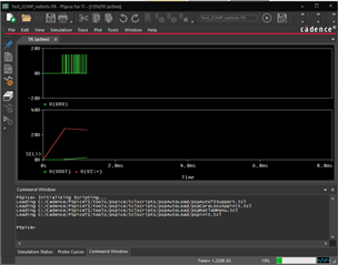
I am start the new design from the UCC28730 PSPICE file "slum527zip"
I don't understand why there is a V2 voltage voltage source for VDD? The output will be 0 if I remove V2.
But the will be no external supply to V2 and VDD comes from HV initially and then from the auxiliary output right ?