This thread has been locked.

If you have a related question, please click the "Ask a related question" button in the top right corner. The newly created question will be automatically linked to this question.

BQ76930: BQ76930 schematic Review

Part Number: BQ76930
Other Parts Discussed in Thread: TIDA-01093

Hi experts,

BQ76930 is mass production on customer side. Now they have 3 board back from end customer. The failure rate is 3%. There are 2pcs of BQ76930 in this system. All the failure are occur in High battery side(11~20 cell). 

Could you review the schematic for customer? So we can propose a method to optimize the design. Thanks.

We think high side BQ76930 was broken for a reason, is there any power up flow for battery? Otherwise, customer didn't place TVS. 

What we did: 

Resistance test: 

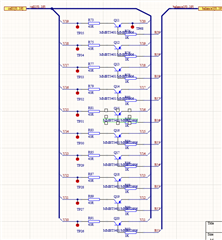
Failure board 1. Failure in cell 16 and cell 17----Back Cell data: Cell 16: 0V; Cell 17: 3.8V

When we take high side BQ76930 down from the board, we find the resistance between Pin20(VC6) and Pin 21(VC5B) is 1.2ohm. 

Failure board 2/3. Failure in cell 11and cell 12----Back Cell data: Cell 16: 0V; Cell 17: 3.8V

Replacement test --- Change a new BQ76930, all the test is fine, BQ76930 can work well

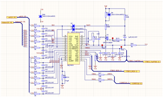
High side BQ76930 Schematic: 

Best Regards

Songzhen Guo

  • Hi Songzhen,

    The reference design for 20 cells we have is TIDA-01093, it does use a TVS across the cell inputs, but I don't know if it would help the situation you describe.  Random cell connection considerations for a single part are shown in the application note https://www.ti.com/lit/pdf/slua749.  Figure 21 shows a condition which may result in a large voltage on VC16 or differential voltage for VC6 vs VC5B.  In the stacked design the lower device filter capacitors may be holding the V10 low while C35 holds VC5x of U3 low.  This might cause the type damage you describe.  The Zeners shown in figure 21 can limit the voltages to those pins above the group power pin.  Connecting the cells bottom up or one 5-cell group at a time from the bottom may reduce the voltage steps to the part and reduce the chance of the damage you describe. 

    In the schematic the topology looks correct, the Cf capacitors (C29 and C35) are recommended to be 10 uF and the Rf and Rc resistors 1k to keep the part alive during SCD conditions, certainly more important on the bottom device which typically monitors current. With the Cc capacitors 1 uF you can see voltage errors during cell balancing, so those capacitors are sometimes smaller.  Both of those value changes would allow more voltage distribution on the inputs during random cell connection, so the Zeners in figure 21 or a connection sequence may be more important.