This thread has been locked.

If you have a related question, please click the "Ask a related question" button in the top right corner. The newly created question will be automatically linked to this question.

LMG1020: Maximum current

Part Number: LMG1020
Other Parts Discussed in Thread: ALLIGATOR

Hi Team, assisting a client.

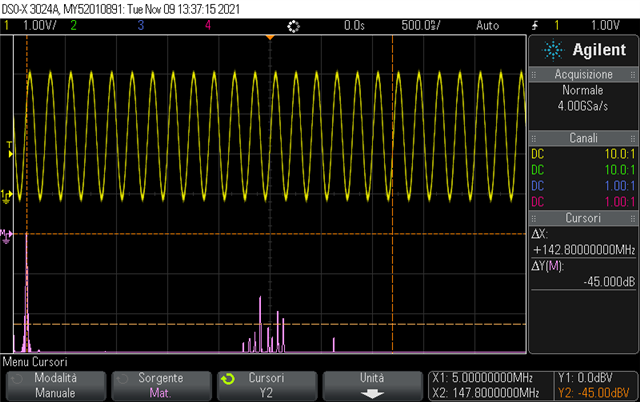
They would like to use the LMG1020 device for switching a GaN device GS66508B at 27.095 MHz (So there is a periodic signal not just one pulse). In the preliminary design, they used 22 Ohm resistors between OUTH, and OUTL (connected in parallel) and the GaN input at the gate.

It seems that these resistances are giving very long charge (OUTL)/discharge (OUTH) time, so at 27.095 MHz the OUTL voltage varies between 0 and 2v, and OUTH varies between 3.6 and 5 v. As a result, the GaN just experiences a slight change in the Q point position and not a complete on/off cycle as it should do.

They are considering to minimize these resistors. However, they am puzzled as to what combination of values could work best for their case. In the LMG1020YFFT data sheet, the OUTL series resistor is "optional". Various references give various values for the values for these resistors, and the series resistors are zero in the evaluation board used here. This could results in significant shortening of time lag if the maximum current values quoted in the LMG102 datasheet are respected.

Hoping for your input.

Thank you.

-Mark

  • Hi Mark,

    Thank you for your question. 22 ohm seems pretty large compared to what I've seen being used in the past. This will slow down their turn on/turn off speed quite a bit, and when using GaN FETs the desire is usually to get fast switching speeds. 

    Here is a guide on how to select the gate resistor value: https://www.ti.com/lit/pdf/slla385?keyMatch=GATE%20RESISTOR%20SELECTION

    In the datasheet we recommend to have at least 2 Ohm resistors. They could also start with 2-3 Ohm, then capture the turn on/turn off signals and adjust based on that. If signal has a lot of ringing they can increase the resistance by 1-2 Ohm until they get a signal that doesn't violate the specification of the device but that is also fast enough for their application.

    Best regards,

    Leslie

  • Hi Leslie, seeking for your further assistance for their response.

    In the meantime, I have done some measurements, and there seems another issue. That is, sort of feedback from OUTH, OUTL outputs to the IN+ input. I will show you the obtained waveform using DSO- X 3024A oscilloscope and N2863B probes, and the alligator ground (I think this should be revised in the next version but here I just show what I have obtained). BTW: All these readings are done just at IN+, and the schematic of the built circuit is shown below this message.

    1. Using a sine signal at IN+ f= 5 MHz, 0-3 v, the time and frequency (FFT) analysis of the signal is shown in Scope_22a screenshot at IN+ of LMG1020 with LMG1020 disconnected from DC supply. As I connect the DC supply, the signal is shown in Scope_22b appears. You can see there is a lot of harmonics (though power-wise they are about -40 dB less, they are strong enough to distort the time domain signal). Given FFT analysis done with 200 MHZ span and 100 MHz-centred screen.
    2. At 5 MHz the time domain signal does not look to be a pure sine at IN+, and there are some “imperfections” as shown in scope_23 when the LMG1020 is on. The amount of these imperfections are quantified using the oscilloscope FFT analysis as shown Scope_22a,b.
    3. Using a sine signal at IN+ f= 30 MHz, 0-3 v, the time and frequency (FFT) analysis of the signal is shown in Scope_24a screenshot at IN+ of LMG1020 with LMG1020 disconnected from DC supply. As I connect the DC supply, the signal is shown in Scope_24b appears.
    4. At 30 MHz the “imperfections” seem to be more powerful as shown in scope_25 when the LMG1020 is on. The amount of these imperfections are quantified using the oscilloscope FFT analysis the same way as before.

    The question is: is there an indication whether the feedback can be avoided/minimised, how can I quantify it, best practices in the layout stage to suppress it, etc.

    /resized-image/__size/640x480/__key/communityserver-discussions-components-files/196/scope_5F00_22a.png

  • Hi Mark,

    Did you mean to attach several images? I can only see image 22a.

    Regards,

    Leslie

  • Hi Mark, 

    Thanks for providing the signals. I'll look into these and get back to you tomorrow.

    Best regards,

    Leslie

  • Hi Mark, 

    I'm a little confused by what you are trying to do here with a sine wave at the input. The driver is design to have a square PWM signal at the input typically from a controller, and that PWM signal defines the ON/OFF state of the driver's output. Typical this PWM signal is driven at only 2 levels: 0V or below VIL to turn OFF the FET and 5V or above VIH to turn ON the FET:

    Regards,

    Leslie