This thread has been locked.

If you have a related question, please click the "Ask a related question" button in the top right corner. The newly created question will be automatically linked to this question.

UCC28740: ucc28740 simplis error support

Part Number: UCC28740
Other Parts Discussed in Thread: TL431

TI,

Starting from the ucc28740 simplis simulation example:

https://www.ti.com/product/UCC28740#design-tools-simulation

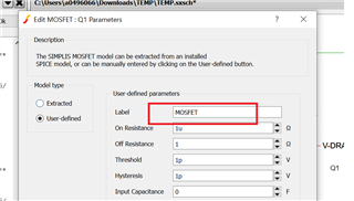
I created a primary (DC input, switch, clamp, bleeder, etc.), auxiliary (to power the ucc28740) and secondary (power output only), copy and pasted the ucc28740 "symbol" then employed the "F11" key to copy and paste the ucc28740 "sub-circuit code" into my new simplis simulation/schematic/file (see attached - not sure if it attached).

Problem:
I am getting a set of errors that do not make any sense (to me):

Errors:

****************************************

<<<<<<<< Error Message ID: 1051 >>>>>>>>

input file C:/Users/dekk0/Desktop/ECEN/9_5527 PE Lab 2/4_Homework/20_Final Design Files/2_Simulations/SIMPLIS_Data/1_PRI_AUX_NO_Cntrls.deck, line 3385:

+ X3= 1.123456789 Y3= 1.123456789

The value of Y3 should be

larger than the value of

Y2 for this device/model.

On SIMetrix/SIMPLIS , Version : 8.50a

*** END SIMPLIS ERROR REPORT ***

First, there is no "line 3385" in the file "SIMPLIS_Data/1_PRI_AUX_NO_Cntrls.deck".

Second, I have no idea what X3 nor Y3 is nor where they are located nor how to begin to resolve this issue.

Would someone please help me resolve this (and I am guessing follow-on) issue(s)?

Thank you,

C

  • Hi, Craig:

    Thank you for asking. 

    I did not see the attachment. Would you please try to upload it again?

    Regards,

    Wesley

  • Hi, Craig:

    I just tried this way and it could operate well. So there would be some issue when you copy/paste the subckt code. 

    My steps are

    1.  File --> New SIMPLIS file. 

    2. Select All and copy in "UCC28740 transit", and pasted them in new SIMPLIS file. 

    3. Copy the SUBCKT code of UCC28470, HVFET, and TL431; Paste them into NEW SIMPLIS (Press F11)

    4. Choose the "Simulator" and execute the transient analysis. It works normally. 

    I am not sure what problem that you meet. Would you please try it again?

    Thanks. 

    Regards, 

    Wesley

  • How does one post simplis simulation files to this board?

  • Hi, Craig:

    You could use the "insert" --> "image/vedio/file" to attach the file in your post. 

    https://e2e.ti.com/cfs-file/__key/communityserver-discussions-components-files/196/UCC28740_5F00_TRANS_5F00_SIMPLIS.sxsch

  • 1_PRI_AUX_NO_Cntrls.zip

    Wesley,

    Ok, took a while to figure out your file upload system (no very obvious - you need to add an official looking "upload" button and add a comment that you only accept zip files and I not sure why one has to first type in the file name then search/add it.).

    Note:  The attached is similar to the original ucc28740 simplis simulation example but only contains the primary side, transformer, secondary (power only - no controls) and auxiliary to power the ucc chip.

    To create the file I:

    First built the primary, secondary and auxiliary circuits,

    Second, copied the ucc "symbol" from the ucc sim example to the attached project,

    Third, via the "F11" command I copied the "sub-circuit code" from the original ucc sim example and into the attached project (I removed parts that I am not using).

    With the ucc feedback pin open the ucc should be driving the up to full output power.

    I must be doing something small wrong.

    I have some experience with SIMetrix/SIMPLIS though not enough to resolve this problem.

    Best of luck.

    Thank you,

    C

  • Hi, Craig:

    I think you missed to input the MOSFET label as below. 

    There is no error message after I key it in. Please check the attachment. 

    Thanks. 

     https://e2e.ti.com/cfs-file/__key/communityserver-discussions-components-files/196/1_5F00_PRI_5F00_AUX_5F00_NO_5F00_Cntrls.sxsch

  • Wesley,

    Thank you for the quick response.

    I seem to be having a difficult time with the FET.

    Two questions:

    1.  Does the ucc28470 require a voltage (range 19 to 23V) on VDD to run or can the chip run on only HV?

    Trying to figure out:

    A:  Does this chip have an auto-shutdown feature if VDD is not detected within a certain amount of time,

    B:  Can I simply start/run this chip (drive the MOSFET) with only a low voltage VDD source (trying to skip a high voltage step in my initial debug of my circuit).

    5516.1_PRI_AUX_NO_Cntrls.zip

    2.  So I made your requested mod and the ucc chip started up though the gave voltage was in the micro-volts.  I selected a more appropriate FET (see attached file), "extracted" the model, then switched to "user defined", named it "MOSFET" and I am back to the original error.

    How does one select/add a FET to this circuit without errors?

    Thank you,

    Craig

  • Hi, Craig:

    You're welcome.

    About your questions, 

    1-A: HV would be turned off after VDD reaches 23V and UCC28740 would turn off if VDD drops below its UVLO.  So the answer is "no". UCC28740 can not be powered by HV. VDD is necessary. 

    1-B: Yes, your could start/run this UCC28740 with only a voltage source supplied to VDD pin. You may find the VDD start/stop/operation spec. in its datasheet as below.  Also, UCC28740 model that we shared is for function simulation.  You could find this model also use a PWL voltage source to power on the IC in TI's simulation schematic.

    UCC28740 datasheet

    2.I would check it. It may take some time. I would suggest you if you would like to check UCC28740's function, you may use the MOSFET model that we TI provided in the simulation first. It would be helpful to save your debugging time. 

    Please let me know if you still meet the error message when you used the MOSFET model 

    Have a nice weekend 

    Regards, 

    Wesley.

  • Wesley,

    I just like to clarify your response to 1-A and 1-B:

    General operation of HV start-up:

    When HV (bulk voltage) is available, the HV pin charges the VDD (VDD capacitor) pin up to 19-23V (turn-on UVLO).  At this point the HV start-up function disables and the chip expects the VDD cap/source to continue powering the circuit.  If the VDD cap/source fails (drops below turn-off UVLO, 7.35 - 8.15V) then the chip shuts down.

    So there is no official shut down timer minus the one created in the size of VDD capacitor chosen and ucc load.

    To be clear, one (in real life) may start the chip by only externally supplying turn-on UVLO (19-23V) to the VDD pin.  Under this condition one should able to watch the chip attempt to drive the gate of the FET.

    Should I be able to replicate via simulation?

    Thank you,

    C

  • Hi, Craig:

    Yes, there is no shut down timer in IC. You may use Irun ( on page 5 in datasheet) and UVLO to calculate the necessary CVDD based on the time you need

    You may start up the chip by supply VDD voltage directly, and of course it could be replicate via SIMPLIS model. If you take a look into the transient model that TI provided. It also supply VDD by external PWL voltage source to turn on this chip. 

    Regards, 

    Wesley

  • Hi, Craig:

    I checked your SIMPLIS file. I thought the error mainly comes from the incorrect schematic. Such as improper MOSFET driver circuit, floating FB and incorrect snubber (or clamping circuit). I made some modification as below. It can simulate without error. However, I have to say this model does not work well because my purpose is just to fix the error. I did not optimize it. 

    My suggestion is that you may run some simulation and modify model TI provided first. It would help you to be familiar with the IC functions and external circuits, and you may save time when you made your own circuit.

    https://e2e.ti.com/cfs-file/__key/communityserver-discussions-components-files/196/1_5F00_PRI_5F00_AUX_5F00_NO_5F00_Cntrls_2D00_modify.sxsch

    Regards, 

    Wesley

  • Wesley,

    Thank you so much for getting this simulation going!

    I see that you added the recommended "Ccs" pin.

    I am guessing that you removed the "HV" connection and added the voltage source to the "V_AUX" / VDD pin to simulate my lab low voltage test experience.

    Note 1:  I replaced your PWL voltage source with a constant 23V to speed things up.

    I understand why you placed the cap on the "FB" pin to prevent a floating condition.

    I understand why you updated my AUX cap from 100 nF to 10 uF (that was a copy and paste mistake).

    I understand that in this open-loop, "max drive" scenario the output (sec and aux) voltages should drive up to some max value.  Not ideal though this is better than where I was a day ago.

    Note 2:  I changed my "Rs2" value from 26.7 kohms to 26.l kohms to better meet the max "VS" limits : 4.52-4.7x V.

    Note 3:  I changed the "Rs2" from 26.7 kohms to 5 kohms to see if I can get the output to a steady state even in this open-loop "max drive" scenario.

    I also made a "__HV start" version (HV pin connected to VBULK and ext V_AUX voltage source removed) and it appears to start as and transition expected!

    I also cleaned up the simulation "sheets" to make thins a little easier to read.

    Questions:

    1.  Why did you add the 100 ohm DRV to Gate resistor?  I do not see that as a recommendation (even in the Layout Example),

    Thank you,

    C

  • Hi, Craig:

    It's very glad to hear your simulation meets your expectation. 

    About the ON resistance, frankly speaking, I added it based on my experience. Normally it is suitable for most of MOSFETs. 

    This resistance is more related to MOSFET's characteristic. The higher resistance would increase the MOSFET switching loss but provides less VDS/VGS ringing, in the other hand, smaller resistance provides better efficiency but higher noise comes from MOSFET di/dt. Generally we would design a simple driver circuit with 2 resistors and 1 diode to driver MOSFET. It is helpful to optimize MOSFET's performance. 

    So, if you would like understand more about MOSFET driver circuit, you could refer the link as below. It would make you more clear about MOSFET's driver circuits. 

    Fundamentals of MOSFET and IGBT Gate Driver Circuits

     Regards, 

    Wesley

  • Wesley,

    Attached primary, secondary and auxiliary HV start (HV start -> run) pics.

    In "HV_start_PRI" the FET appears to be conducting a lot more current (expecting < 2 A max) and the gate voltage appears to be a lot higher than expected (14 V max).

    Question 1:

    Should one expect these levels given this setup?

    In "HV_start_AUX", after HV start turns off (roughly 14 ms) it appears as though either the VDD pin is powering the auxiliary winding with about 400 mA or the VDD pin is consuming a 400 mA (the "inline current probe" is pointing in the direction of VDD pin power auxiliary).

    Question 2:

    Does this seem right?  If the Q of the FET is very very high then one would expect the chip to draw more drive current though I thought that the chip was limited to 25 mA.

    HV_start_pics.zip

    Thank you,

    C

  • Wesley,

    I think I need a little clarity on setting of the RS1 and RS2 values.

    First, I need the system to work over the following input range: 85 to 264 VRMS

    RS1 equation = Vin(run)*sqrt(2)/(NPA*IVSL(run)

    For my system NPA = NPS = 8, ok

    VIN(run) = AC RMS voltage to enable turn-on of the controller = 85 VRMS, ok

    IVSL(run) = 190 (min), 225(nom), 275(max) uA: 

    Question 1:

    Do I need to figure out which value my actual chip is using (derive somehow) or do I pick one to work with some range - for example is there a better value for my required input voltage range?

    RS2 equation = (RS1*VOVP)/(NAS*(VOV-VF)-VOVP)

    For my system NA = NS so NAS = 1, ok

    VOV = maximum allowable peak voltage at the converter output

    Question 2:

    Is this a peak voltage (max peak current *cap esr + max steady-state or max steady-state or max steady-state plus some fudge factor?

    VF = output-rectifier forward drop at near-zero current? 

    Question 3:

    Is this referring to the input AC rectifier diode voltage or auxiliary rectifier diode voltage?

    VOVP = 4.52 (min), 4.36(nom), 4.71(max),

    Question 3:

    Do I need to figure out which value my actual chip is using (derive somehow) or do I pick one to work with some range - for example is there a better value for my required input voltage range?

    Thank you,

    C

  • Hi, Craig:

    Please check my reply as below. 

    In "HV_start_AUX", after HV start turns off (roughly 14 ms) it appears as though either the VDD pin is powering the auxiliary winding with about 400 mA or the VDD pin is consuming a 400 mA (the "inline current probe" is pointing in the direction of VDD pin power auxiliary).

    Does this seem right?  If the Q of the FET is very very high then one would expect the chip to draw more drive current though I thought that the chip was limited to 25 mA.

    It is strange waveform. You could zoom in and look into its detail to make sure its direction. both of these 2 questions need to more information to check if they are correct.

    Do I need to figure out which value my actual chip is using (derive somehow) or do I pick one to work with some range - for example is there a better value for my required input voltage range? -IVSL(run) = 190 (min), 225(nom), 275(max) uA: 

    It depends on your system request. These 3 value are used to estimate the distribution when the system mess production. Usually we pick the typical value to calculate the R1, and put the R1 value back into the equation to calculate Vin(run) range. For example,  through the calculation, R1 is 535Kohm (based on 85Vac, IVSL=225mA). The start-up Viin range would be 71.1V~103.8V when you system goes to mess production. 

    Question 2:

    Is this a peak voltage (max peak current *cap esr + max steady-state or max steady-state or max steady-state plus some fudge factor?

    I do not quite understand your question. Are you asking the VOV's definition?

    IC senses the output voltage through aux wilding. VOV is not for steady state. It is a system fault condition. For example, if something happens in feedback loop to make IC can not sense FB signal through photo, FB goes high and it causes output voltage is over 12V. VOV is the max limitation to protect component on 2nd side. i.e output cap. If the output cap is only 16Vmax, the VOV must be smaller than 16V. but higher than 12V.

    Question 3:

    Is this referring to the input AC rectifier diode voltage or auxiliary rectifier diode voltage?

    VOVP = 4.52 (min), 4.36(nom), 4.71(max),

    The answer is similar to the IVSL one. it is same concept when we are in design stage.

    Regards,

    Wesley

  • Hi, Craig:

    I saw the notification but it seems your post is deleted. Hope your question is solved. 

    let me know if you meet assistance or you could open another thread to further discussion. 

    Regards.

    Wesley